An ASIP architecture framework to facilitate automated
design space exploration and synthesis for Iterative Repair
solvers
Aravind Dasu and Jonathan Phillips
Electrical and Computer Engineering
Utah State University
4120 Old Main Hill
Logan, UT 84321 USA
Abstract-Autonomous dynamic event scheduling, using
Iterative Repair techniques such as those employed by CASPER
and ASPEN, is an essential component of successful space
missions, as it enables spacecraft to adaptively schedule tasks in a
dynamic, real-time environment. Event rescheduling is a
compute-intensive process. Typical applications involve
scheduling hundreds of events that share tens or hundreds of
resources. We are developing a set of tools for automating the
derivation of application-specific processors (ASIPs) from ANSI
C source code that perform this scheduling in an efficient
manner. The tools will produce VHDL code targeted for a Xilinx
Virtex 4 FPGA (Field Programmable Gate Array). Features of
FPGAs, including large processing bandwidth and embedded
ASICs and block RAMs, are exploited to optimize the design.
Efficiency is measured by combining the factors of execution
speed, circuit size, power consumption, and fault tolerance.
Iterative Repair problems are generally solved using a
combinatorial search heuristic, such as Simulated Annealing
(which is used by CASPER and ASPEN), Genetic Algorithms, or
Stochastic Beam Search. All of these methods operate by
gradually improving an initial solution over hundreds or
thousands of iterations. We propose an FPGA-based
architectural framework derived from ANSI C function-level
blocks for accelerating these computations. At a function level,
99% of the work done by any Simulated Annealing algorithm is
the repeated execution of three high-level steps: (1) generating a
new solution, (2) evaluating the solution, and (3) determining
whether the new solution should be accepted. The specifics of
how each step operates vary with the application and are
implemented in VHDL through data- and control-flow analysis
of the source C code. In this paper, we discuss specifics of an
architecture template for automated processor design.
I. INTRODUCTION
Field Programmable Gate Arrays (FPGAs) are becoming
increasingly popular as a platform of choice for spacecraft
computer systems. FPGA-based designs are highly cost
effective compared to Application-Specific Integrated Circuits
(ASICs), and provide more computing power and efficiency
than standard microprocessors. Current and planned NASA
missions that utilize FPGA technology include MARTE (Mars
Astrobiology Research and Technology Experiment) [1] and
the Discovery and New Frontier programs [2]. However, the
complexity of designing even reasonably efficient micro-
architectures on commodity FPGA devices is daunting for
engineers outside the realm of VLSI design.
Therefore, a methodology for automatic derivation of
FPGA-based application-specific processors for use in the
mission planning and event scheduling computations
performed by satellites and deep-space probes will mitigate
this steep barrier and facilitate their adoption to a larger
audience who do not have skills in VLSI design. Through our
methodology custom ASIPs on FPGAs can quickly be
designed which exploit the features of the scheduling
algorithms and maximize the efficiency of the system.
II. RELATED WORK
Our methodology leverages concepts from several different
research areas, including hardware implementations of
heuristic search techniques, the design of application-specific
instruction processors (ASIPs), and methods for performing
design space exploration for FPGA-based processors. Recent
advances in each of these fields are discussed in this section.
Iterative repair utilizes a combinatorial search heuristic,
such as a genetic algorithm (GA), simulated annealing (SA),
or a stochastic beam search (SBS), to arrive at a solution. In
theory, implementing these combinatorial search algorithms in
hardware could significantly speed up the search process.
Large amounts of parallelism and pipelining can be extracted
from GA and SBS, since deriving a new generation is largely
only a function of the previous generation.
FPGA-based GAs and SBS have been implemented for the
purposes of blind signal separation [3], filter design [4],
function interpolation [5], and speech recognition [6]. As long
as the solution length is kept reasonably small, this technique
in which entire solutions are passed between pipelined
modules works well. Iterative repair problems, however, are
complex enough that a solution can be hundreds of bytes in
length.
Design space exploration in the context of FPGA-based
architectures is a powerful tool. Exploring a design space is,
in essence, searching the combinatorial space of all possible
hardware architectures that can support a given function. The
goal is to identify the architecture that yields the best tradeoff

between conflicting goals, such as minimizing required FPGA
resources while maximizing system throughput. The design
space is generally very large, thus demanding a search
heuristic such as simulated annealing or a genetic algorithm to
arrive at a solution within a reasonable amount of time. An
FPGA design space can be searched at many levels, from the
low-level specification of individual look-up tables to high-
level complex modules.
An overview of the different types of processors that are
typically considered in a design space search is provided in [7].
Reduced Instruction Set (RISC), Complex Instruction Set
(CISC), VLIW (Very Long Instruction Word), dataflow, and
tagged-token architectures are all commonly utilized. A
design space explorer is generally restricted to one flavor of
processor in order to put an upper bound on the time needed to
search the design space. Trying to search across all possible
architectures is considered to be an intractable problem.
In [8], a good description of performing design space
exploration for a reconfigurable processor is described.
Important elements to be considered in the design space
include allocation of computational, control, and memory
resources, along with the scheduling of operations onto these
resources. Exploration can occur in both parallelization
(spatial optimization) and pipelining (temporal optimization).
Simulated annealing is employed as the search heuristic. Over
thousands of iterations of the simulated annealing algorithm,
the throughput of the algorithm gradually improves.
III. IMPLEMENTATION
In order to develop an automated tool to derive a micro-
architecture from a C program describing applications within
the class of iterative repair based scheduling algorithms
similar to that shown in fig. 1, we are taking the approach of
first defining and prototyping an application oriented
architecture framework. This framework will then be used to
guide the tool to analyze the C program and determine the
specifics of different control, memory, and computation
modules that make up the application-specific processor. The
general hardware framework consists of an architecture that is
conducive to the execution of the simulated annealing
algorithm as employed by Iterative Repair. Based upon the
framework shown in fig. 1, a tool flow is derived for the
design of iterative repair processors. This tool flow is shown
in fig 2. Source C code for an Iterative Repair problem is first
passed through GCC to obtain an intermediate .cfg format.
This is then passed through an Intermediate Format Generator
to produce custom Control-Data flow graphs. The custom
CDFGs are then partitioned by function to Design Space
Explorers for the different pipeline stages. The Design Space
Explorers take the Intermediate Format code a stage-specific
architecture template, and a constraint file, and produce an
architecture for each pipeline stage. In this paper, we
specifically discuss the custom intermediate code and the
templates that have been derived for each stage.
In a simulated annealing/iterative repair technique solutions
are represented as a string of start times for events numbered 0
to n-1 for a problem consisting of n events that need to be
scheduled. Lists of available resources and resources needed
by each event are also provided. A generic framework macro-
architecture for such algorithms is shown in fig 3.
The architecture is composed of a five-stage pipeline
coupled with six memory banks. A global controller
coordinates execution and data exchange between the units.
As this is a pipelined architecture, it can only operate as fast as
the slowest stage. Design Space Exploration techniques must
be employed in the more complex stages to minimize the
latency. Each of these stages is discussed in detail in this
section.
A. Memory Design
The architecture consists of 6 memory banks, derived from
Xilinx FPGA block RAMs. A 1024-word (32-bit word)
memory bank consumes 4 BRAMs. Each memory bank holds
a solution, the score of the solution, and provides some space
for temporary data storage. At a given point in time, one
Figure 1: Pseudocode for the Simulated Annealing algorithm. The main
loop consists of five steps.
Figure 2: High-level diagram showing tool flow from C source code to
application-specific architecture. Red text indicates portions discussed
in this paper

memory bank is associated with each of the five processing
stages in the pipeline. The sixth memory block holds the best
solution found so far. The main controller determines how
memory blocks are associated with different processing stages.
Details on the manner in which memory banks are managed
are discussed in the section on the main controller.
B. Copy Processor
As shown in fig. 1, the main loop of the simulated annealing
algorithm begins by making a copy of the best solution. This
copy is then altered to generate a new solution that could
potentially replace the best solution. In the architecture shown
in fig. 3, the Copy Processor performs this function.
Assuming the length of the solution is known; the contents
of the solution in the “best-solution” memory bank are copied,
word by word, into the memory bank currently associated with
the Copy Processor. There is no need to accelerate the copy
process, as this pipeline stage is guaranteed to complete in
n+1 clock cycles for a solution length of n. Other stages are
much more compute-intensive. As can be seen from fig. 4, the
copy processor is merely a controller to facilitate data
transfers. The “step” signal comes from the main controller,
indicating that a new pipeline step has begun. The copy
controller consists of a counter that generates addresses and
produces a “done” signal when all data has been copied and
also controls the write-enable line on the destination memory
bank. The source and destination addresses are identical,
because the data locations in each memory bank are identical.
C. Alter Processor
The second stage in the Iterative Repair pipeline is the Alter
Processor. The C code for this function is as follows:
void alter(int *sched)
{
int i, j;
i = rand() % MAX_EVENTS;
j = rand() % MAX_LATENCY;
sched[i] = j;
}
Basically, one event is selected at random from the solution
string. The start time of this event is changed to a random
value smaller than the maximum latency. This stage shown in
fig. 5 could be accelerated by introducing an additional
random number generator and an additional divider, allowing
for maximum concurrency. But it is not necessary as a 15-
cycle integer divider allows this stage to terminate in 21 clock
cycles, regardless of the size of the solution string. As
solutions generally consist of hundreds of events, even the
simple Copy Processor will have a greater latency than the
Alter Processor. The alter controller is based on a counter that
starts when the “step” signal is received from the Main
Controller, control logic to enable register writing on the
“address” and “data” registers on the proper clock cycles, and
a “done” signal to indicate that the stage has completed.
D. Accept Processor
The Accept Processor’s job is to determine whether to
accept the current solution as the new best solution. If the
Figure 3: Top-level architecture depiction for a pipelined Iterative Repair
processor. Black lines represent data buses and red lines signify control
signals.
Figure 4: The Copy Processor: Data is copied word by word from the
source memory bank to the destination memory bank.
Figure 5. The Alter Processor. A random number generator is used to
modify the incoming solution.

current solution is better than the best solution, the current
solution is accepted unconditionally. According to the
Simulated Annealing algorithm, a solution that is worse than
the best solution can also be accepted with a computed
probability, defined in (1).
p = e
∆E/T
, ∆E = S
cur
- S
best
(1)
S
cur
and S
best
are the current and best scores, respectively,
and T represents temperature. This probability is a function of
both the temperature and the difference between the score of
the current solution and the score of the new solution. When
the temperature is high, suboptimal solutions are more-likely
to be accepted. This feature allows the algorithm to escape
from local minima as it searches the solution space and zero in
on the true optimal solution.
An architecture that supports this computation is shown in
fig 6. The best score and the current score are read from their
respective memory banks. The temperature is provided by the
Main Controller. The random number generator (RNG) is a
simple 15-bit tapped shift register. The exponential block is a
BRAM-based lookup table. The I-to-F block is an integer-to-
float converter.
E. Adjust Temperature Processor
The Adjust Temperature Processor is a simple but critical
stage in the pipelined processor. The temperature is used to
compute the probability of acceptance in the Accept Processor
and by the Main Controller to determine when the algorithm
should complete. The architecture for the Adjust Temperature
Processor is shown in fig. 7. The current temperature is stored
in a register. When the “step” signal is received, the
temperature is multiplied by the constant “cooling rate”,
which is typically a value such as 0.9999. This cooling rate
allows the temperature to decrease slowly and geometrically,
allowing for the discovery of better solutions.
F. Main Controller
The main controller keeps track of the memory block that is
associated with each processing stage. Upon the completion
of a pipeline period, the main controller must determine how
to reassign the memory blocks to the different stages, keeping
track of which one holds the best solution and which one can
be recycled and assigned to the Copy Processor. The main
controller also performs global synchronization. As shown in ,
the main controller receives a “done” signal from each of the
pipeline stages. When all stages have completed, the main
controller sends out a “step” signal to each processor,
indicating that they can proceed. The main controller also
monitors the temperature and halts the system when the
algorithm is complete.
G. Evaluate Processor
The Evaluate Processor is by far the most complex of all the
pipeline stages in the Iterative Repair architecture. Work is
currently in progress for designing this stage. The “score” of a
solution to the Iterative Repair problem consists of 3
components. A penalty is incurred for total clock cycles
consumed by the schedule. A penalty is assessed for double-
booking a resource on a given clock cycle. Also, a penalty is
assigned for dependency violations, which occur when event
“b” depends upon the results of event “a”, but event “b” is
scheduled before event “a”.
Fig. 8 shows an intermediate output of our tool as it works
upon the Evaluate Processor. Fig. 7 is a control-data flow
Figure 7: Adjust Temperature Processor. The temperature is reduced
geometrically each time this processing stage runs.
Figure 6: The Accept Processor. The new solution is always accepted if it
is better. If worse, it is accepted with a computed probability.
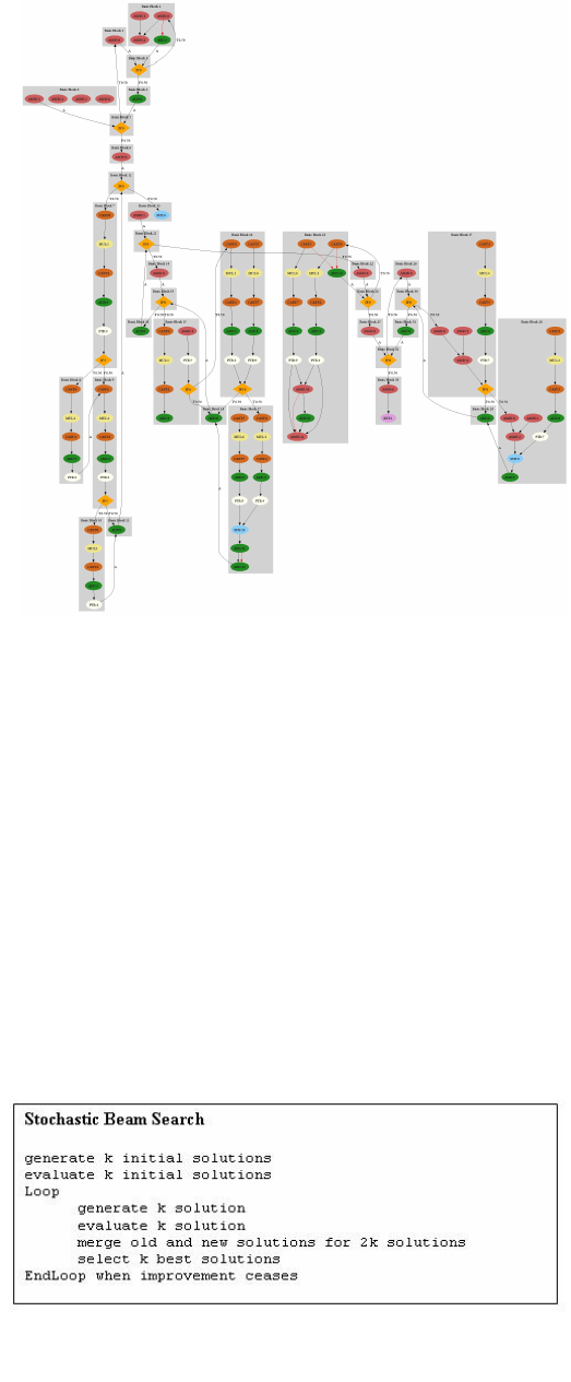
graph depicting basic blocks, data dependencies, control
dependencies, and data operations for the evaluate function
described above. The Evaluate Processor will be designed
using Design Space Exploration. A Simulated Annealing
heuristic will be utilized to identify the optimal processor. In
this case, optimal signifies the appropriate tradeoff between
latency of the Evaluate Processor and resource utilization on
the FPGA.
The manner in which the design space is searched is as
follows: A minimally adequate architecture is derived as a
starting point for the processor. The search is performed by
repeatedly increasing the resources (such as arithmetic units or
temporary register storage) allotted to the Evaluate Processor
to reduce its latency until either no further optimization can be
done or the processor latency falls below the latency of
another processing stage. Latency is determined by
simulating the performance of the processor using a software
model.
IV. FUTURE WORK
The first priority for future work is to complete the Evaluate
Processor. The entire architecture can then be tested and
optimized. The end-to-end tool chain depicted in fig. 2 can
then be built.
The architecture described in this paper is only an initial
stage in our vision of hardware acceleration of the Iterative
Repair algorithm. Once the processing platform outlined here
has been completed, a future step would be to further exploit
the parallel nature of the iterative repair algorithm. Simulated
Annealing is a sequential algorithm that can be pipelined, but
not parallelized. However, similar heuristic search techniques
exist that are much more conducive to parallelization.
Stochastic Beam Search is one of these. It is almost identical
to Simulated Annealing, but a set of “best” solutions are
maintained, rather than a single solution. The pseudocode for
the Stochastic Beam Search is shown in fig. 9. A modified
version of the Stochastic Beam Search could better utilize
FPGA resources if significant space is left by the traditional
Simulated Annealing algorithm.
Finally, the tool will be designed to accept additional
optimization constraints such as using Triple Modular
Redundancy (TMR) or other techniques for implementing
fault tolerance along with power optimization strategies.
REFERENCES
[1] A. Winterholler, M. Roman, D. Miller, J. Krause, and T. Hunt,
"Automated core sample handling for future Mars drill missions," in 8th
International Symposium on Artificial Intelligence, Robotics and
Automation in Space Germany, 2005.
[2] "New Space Communications Capabilities Available for NASA's
Discovery and New Frontier Programs," in NASA Technology
Discovery/New Frontier Roadmap, 2006.
[3] H. Emam, M. A. Ashour, H. Fekry, and A. M. Wahdan, "Introducing an
FPGA based genetic algorithms in the applications of blind signals
separation," in System-on-Chip for Real-Time Applications, 2003.
Proceedings. The 3rd IEEE International Workshop on, 2003, pp. 123-
127.
[4] M. S. Hamid and S. Marshall, "FPGA realisation of the genetic
algorithm for the design of grey-scale soft morphological filters," in
Visual Information Engineering, 2003. VIE 2003. International
Conference on, 2003, pp. 141-144.
[5] H. E. Mostafa, A. I. Khadragi, and Y. Y. Hanafi, "Hardware
implementation of genetic algorithm on FPGA," in Radio Science
Conference, 2004. NRSC 2004. Proceedings of the Twenty-First
National, 2004, pp. C9-1-9.
[6] T. Anantharaman and R. Bisiani, "A hardware accelerator for speech
recognition algorithms," in Proceedings of the 13th annual international
symposium on Computer architecture, Tokyo, Japan, 1986, pp. 216-223.
[7] G. Mehta, R. R. Hoare, J. Stander, and A. K. Jones, "Design space
exploration for low-power reconfigurable fabrics," in Parallel and
Distributed Processing Symposium, 2006. IPDPS 2006. 20th
International, 2006, p. 4 pp.
[8] B. Miramond and J. M. Delosme, "Design space exploration for
dynamically reconfigurable architectures," in Design, Automation and
Test in Europe, 2005. Proceedings, 2005, pp. 366-371 Vol. 1.
Figure 8: Control-Data Flow Graph of the Evaluate function. Information
contained in this graph can be used to create an optimal application-specific
processor.
Figure 9. The Stochastic Beam Search algorithm is similar to
Simulated Annealing.
