
Intel
®
Architecture
Instruction Set Extensions
and Future Features
Programming Reference
March 2024
319433-052

Document Number: 319433-052 ii
Notices & Disclaimers
This document contains information on products in the design phase of development. The information here is
subject to change without notice. Do not finalize a design with this information.
Intel technologies may require enabled hardware, software or service activation.
No product or component can be absolutely secure.
Your costs and results may vary.
You may not use or facilitate the use of this document in connection with any infringement or other legal analysis concerning
Intel products described herein. You agree to grant Intel a non-exclusive, royalty-free license to any patent claim thereafter
drafted which includes subject matter disclosed herein.
All product plans and roadmaps are subject to change without notice.
The products described may contain design defects or errors known as errata which may cause the product to deviate from
published specifications. Current characterized errata are available on request.
Intel disclaims all express and implied warranties, including without limitation, the implied warranties of merchantability,
fitness for a particular purpose, and non-infringement, as well as any warranty arising from course of performance, course of
dealing, or usage in trade.
Code names are used by Intel to identify products, technologies, or services that are in development and not publicly
available. These are not “commercial” names and not intended to function as trademarks.
No license (express or implied, by estoppel or otherwise) to any intellectual property rights is granted by this document, with
the sole exception that a) you may publish an unmodified copy and b) code included in this document is licensed subject to
the Zero-Clause BSD open source license (0BSD), https://opensource.org/licenses/0BSD. You may create software
implementations based on this document and in compliance with the foregoing that are intended to execute on the Intel
product(s) referenced in this document. No rights are granted to create modifications or derivatives of this document.
© Intel Corporation. Intel, the Intel logo, and other Intel marks are trademarks of Intel Corporation or its subsidiaries. Other
names and brands may be claimed as the property of others.

Document Number: 319433-052 iii
Revision History
Revision Description Date
-025
• Removed instructions that now reside in the Intel
®
64 and IA-32
Architectures Software Developer’s Manual.
• Minor updates to chapter 1.
• Updates to Table 2-1, Table 2-2 and Table 2-8 (leaf 07H) to indicate
support for AVX512_4VNNIW and AVX512_4FMAPS.
• Minor update to Table 2-8 (leaf 15H) regarding ECX definition.
• Minor updates to Section 4.6.2 and Section 4.6.3 to clarify the effects of
“suppress all exceptions”.
• Footnote addition to CLWB instruction indicating operand encoding
requirement.
• Removed PCOMMIT.
September 2016
-026
• Removed CLWB instruction; it now resides in the Intel
®
64 and IA-32
Architectures Software Developer’s Manual.
• Added additional 512-bit instruction extensions in chapter 6.
October 2016
-027
• Added TLB CPUID leaf in chapter 2.
• Added VPOPCNTD/Q instruction in chapter 6,and CPUID details in
chapter 2.
December 2016
-028 • Updated intrinsics for VPOPCNTD/Q instruction in chapter 6. December 2016
-029
• Corrected typo in CPUID leaf 18H.
• Updated operand encoding table format; extracted tuple information
from operand encoding.
• Added VPERMB back into chapter 5; inadvertently removed.
• Moved all instructions from chapter 6 to chapter 5.
• Updated operation section of VPMULTISHIFTQB.
April 2017
-030
• Removed unnecessary information from document (chapters 2, 3 and 4).
• Added table listing recent instruction set extensions introduction in Intel
64 and IA-32 Processors.
• Updated CPUID instruction with additional details.
• Added the following instructions: GF2P8AFFINEINVQB, GF2P8AFFINEQB,
GF2P8MULB, VAESDEC, VAESDECLAST, VAESENC, VAESENCLAST,
VPCLMULQDQ, VPCOMPRESS, VPDPBUSD, VPDPBUSDS, VPDPWSSD,
VPDPWSSDS, VPEXPAND, VPOPCNT, VPSHLD, VPSHLDV, VPSHRD,
VPSHRDV, VPSHUFBITQMB.
• Removed the following instructions: VPMADD52HUQ, VPMADD52LUQ,
VPERMB, VPERMI2B, VPERMT2B, and VPMULTISHIFTQB. They can be
found in the Intel
®
64 and IA-32 Architectures Software Developer’s
Manual, Volumes 2A, 2B, 2C, & 2D.
• Moved instructions unique to processors based on the Knights Mill
microarchitecture to chapter 3.
• Added chapter 4: EPT-Based Sub-Page Permissions.
• Added chapter 5: Intel
®
Processor Trace: VMX Improvements.
October 2017

Document Number: 319433-052 iv
-031
• Updated change log to correct typo in changes from previous release.
• Updated instructions with imm8 operand missing in operand encoding
table.
• Replaced “VLMAX” with “MAXVL” to align terminology used across
documentation.
• Added back information on detection of Intel AVX-512 instructions.
• Added Intel
®
Memory Encryption Technologies instructions PCONFIG and
WBNOINVD. These instructions are also added to Table 1-1 “Recent
Instruction Set Extensions Introduction in Intel 64 and IA-32 Processors”.
Added Section 1.5 “Detection of Intel
®
Memory Encryption Technologies
(Intel
®
MKTME) Instructions”.
• CPUID instruction updated with PCONFIG and WBNOINVD details.
• CPUID instruction updated with additional details on leaf 07H: Intel
®
Xeon Phi™ only features identified and listed.
• CPUID instruction updated with new Intel
®
SGX features in leaf 12H.
• CPUID instruction updated with new PCONFIG information sub-leaf 1BH.
• Updated short descriptions in the following instructions: VPDPBUSD,
VPDPBUSDS, VPDPWSSD and VPDPWSSDS.
• Corrections and clarifications in Chapter 4 “EPT-Based Sub-Page
Permissions”.
• Corrections and clarifications in Chapter 5 “Intel® Processor Trace: VMX
Improvements”.
January 2018
-032
• Corrected PCONFIG CPUID feature flag on instruction page.
• Minor updates to PCONFIG instruction pages: Changed Table 2-2 to use
Hex notation; changed “RSVD, MBZ” to “Reserved, must be zero” in two
places in Table 2-3.
• Minor typo correction in WBNOINVD instruction description.
January 2018
-033
• Updated Table 1-2 “Recent Instruction Set Extensions / Features
Introduction in Intel® 64 and IA-32 Processors” .
• Added Section 1.4, “Detection of Future Instructions and Features”.
• Added CLDEMOTE, MOVDIRI, MOVDIR64B, TPAUSE, UMONITOR and
UMWAIT instructions.
• Updated the CPUID instruction with details on new instructions/features
added, as well as new power management details and information on
hardware feedback interface ISA extensions.
• Corrections to PCONFIG instruction.
• Moved instructions unique to processors based on the Knights Mill
microarchitecture to the Intel
®
64 and IA-32 Architectures Software
Developer’s Manual.
• Added Chapter 5 “Hardware Feedback Interface ISA Extensions”.
• Added Chapter 6 “AC Split Lock Detection”.
March 2018
-034
• Added clarification to leaf 07H in the CPUID instruction.
• Added MSR index for IA32_UMWAIT_CONTROL MSR.
• Updated registers in TPAUSE and UMWAIT instructions.
• Updated TPAUSE and UMWAIT intrinsics.
May 2018
Revision Description Date

Document Number: 319433-052 v
-035
• Updated Table 1-2 “Recent Instruction Set Extensions / Features
Introduction in Intel® 64 and IA-32 Processors” to list the AVX512_VNNI
instruction set architecture on a separate line due to presence on future
processors available sooner than previously listed.
• Updated CPUID instruction in various places.
• Removal of NDD/DDS/NDS terms from instructions. Note: Previously, the
terms NDS, NDD and DDS were used in instructions with an EVEX (or
VEX) prefix. These terms indicated that the vvvv field was valid for
encoding, and specified register usage. These terms are no longer
necessary and are redundant with the instruction operand encoding
tables provided with each instruction. The instruction operand encoding
tables give explicit details on all operands, indicating where every
operand is stored and if they are read or written. If vvvv is not listed as
an operand in the instruction operand encoding table, then EVEX (or
VEX) vvvv must be 0b1111.
• Added additional #GP exception condition to TPAUSE and UMWAIT.
• Updated Chapter 5 “Hardware Feedback Interface ISA Extensions” as
follows: changed scheduler/software to operating system or OS, changed
LP0 Scheduler Feedback to LP0 Capability Values, various description
updates, clarified that capability updates are independent, and added an
update to clarify that bits 0 and 1 will always be set together in Section
5.1.4.
• Added IA32_CORE_CAPABILITY MSR to Chapter 6 “AC Split Lock
Detection”.
October 2018
-036
• Added AVX512_BF16 instructions in chapter 2; related CPUID
information updated in chapter 1.
• Added new section to chapter 1 describing bfloat16 format.
• CPUID leaf updates to align with the Intel
®
64 and IA-32 Architectures
Software Developer’s Manual.
• Removed CLDEMOTE, TPAUSE, UMONITOR, and UMWAIT instructions;
they now reside in the Intel
®
64 and IA-32 Architectures Software
Developer’s Manual.
• Changes now marked by green change bars and green font in order to
view changes at a text level.
April 2019
-037
• Removed chapter 3, “EPT-Based Sub-Page Permissions”, chapter 4,
“Intel
®
Processor Trace: VMX Improvements”, and chapter 6, “Split Lock
Detection”; this information is in the Intel
®
64 and IA-32 Architectures
Software Developer’s Manual.
• Removed MOVDIRI and MOVDIR64B instructions; they now reside in the
Intel
®
64 and IA-32 Architectures Software Developer’s Manual.
• Updated Table 1-2 with new features in future processors.
• Updated Table 1-3 with support for AVX512_VP2INTERSECT.
• Updated Table 1-5 with support for ENQCMD: Enqueue Stores.
• Added ENQCMD/ENQCMDS and VP2INTERSECTD/VP2INTERSECTQ
instructions, and updated CPUID accordingly.
• Added new chapter: Chapter 4, UC-Lock Disable.
May 2019
Revision Description Date

Document Number: 319433-052 vi
-038
• Removed instruction extensions/features from Table 1-2 “Recent
Instruction Set Extensions / Features Introduction in Intel
®
64 and IA-32
Processors” that are available in processors covered in the Intel
®
64 and
IA-32 Architectures Software Developer’s Manual. This information can
be found in Chapter 5 “Instruction Set Summary”, of Volume 1.
• In Section 1.7, “Detection of Future Instructions”, removed instructions
from Table 1-5 “Future Instructions” that are available in processors
covered in the Intel
®
64 and IA-32 Architectures Software Developer’s
Manual.
• Removed instructions with the following CPUID feature flags:
AVX512_VNNI, VAES, GFNI (AVX/AVX512), AVX512_VBMI2,
VPCLMULQDQ, AVX512_BITALG; they now reside in the Intel
®
64 and
IA-32 Architectures Software Developer’s Manual.
• CPUID instruction updated with Hybrid information sub-leaf 1AH,
SERIALIZE and TSXLDTRK support, updates to the L3 Cache Intel RDT
Monitoring Capability Enumeration Sub-leaf, and updates to the Memory
Bandwidth Allocation Enumeration Sub-leaf.
•Replaced
← with := notation in operation sections of instructions. These
changes are not marked with change bars.
• Added the following instructions: SERIALIZE, XRESLDTRK, XSUSLDTRK.
• Update to the VDPBF16PS instruction.
• Updates to Chapter 4, “Hardware Feedback Interface ISA Extensions”.
• Added Chapter 5, “TSX Suspend Load Address Tracking”.
• Added Chapter 6, “Hypervisor-managed Linear Address Translation”.
• Added Chapter 7, “Architectural Last Branch Records (LBRs)”.
• Added Chapter 8, “Non-Write-Back Lock Disable Architecture”.
• Added Chapter 9, “Intel® Resource Director Technology Feature
Updates”.
March 2020
-039
• Updated Section 1.1 “About this Document” to reflect chapter changes in
this release.
• Added Section 1.2 “DisplayFamily and DisplayModel for Future
Processors”.
• Updated Table 1-2 “Recent Instruction Set Extensions / Features
Introduction in Intel® 64 and IA-32 Processors”.
• CPUID instruction updated.
• Removed Chapter 4 “Hardware Feedback Interface”. This information is
now in the Intel
®
64 and IA-32 Architectures Software Developer’s
Manual.
• Updated Figure 5-1 “Example HLAT Software Usage”.
• Added Table 6-5 “Encodings for 64-Bit Guest-State Fields
(0010_10xx_xxxx_xxxAb)” to Chapter 6.
• Added Chapter 8 “Bus Lock and VM Notify”.
June 2020
-040
• Updated Section 1.1 “About this Document” to reflect chapter changes in
this release.
• Updated Table 1-2 “Recent Instruction Set Extensions / Features
Introduction in Intel® 64 and IA-32 Processors”.
• CPUID instruction updated.
• Added notation updates to the beginning of Chapter 2. Updated ENQCMD
and ENQCMDS instructions to use this notation.
• Added Chapter 3, “Intel® AMX Instruction Set Reference, A-Z”.
• Minor updates to Chapter 6, “Hypervisor-managed Linear Address
Translation”.
June 2020
Revision Description Date

Document Number: 319433-052 vii
-041
• Updated Section 1.1 “About this Document” to reflect chapter changes in
this release.
• Updated Table 1-2 “Recent Instruction Set Extensions / Features
Introduction in Intel® 64 and IA-32 Processors”.
• CPUID instruction updated for enumeration of several new features.
• PCONFIG instruction updated.
• Added CLUI, HRESET, SENDUIPI, STUI, TESTUI, UIRET, VPDPBUSD,
VPDPBUSDS, VPDPWSSD, and VPDPWSSDS instructions to Chapter 2.
• Updated Figure 3-2, “The TMUL Unit”.
• Update to pseudocode of TILELOADD/TILELOADDT1 instruction.
• Addition to Section 6.2, “VMCS Changes”.
• Update to Section 7.1.2.4, “Call-Stack Mode”.
• Update to Section 9.1 “Bus Lock Debug Exception”.
• Added Chapter 11, “User Interrupts”.
• Added Chapter 12, “Performance Monitoring Updates”.
• Added Chapter 13, “Enhanced Hardware Feedback Interface”.
October 2020
-042
• CPUID instruction updated.
• Removed the following instructions: VCVTNE2PS2BF16,
VCVTNEPS2BF16, VDPBF16PS, VP2INTERSECTD/VP2INTERSECTQ, and
WBNOINVD. They can be found in the Intel
®
64 and IA-32 Architectures
Software Developer’s Manual, Volume 2C.
• Updated bit positions in Section 6.12, “Changes to VMX Capability
Reporting”.
• Typo correction in Chapter 8, “Non-Write-Back Lock Disable
Architecture”.
• Several updates to Chapter 13, “Enhanced Hardware Feedback Interface
(EHFI)”.
• Added Chapter 14, “Linear Address Masking (LAM)”.
• Added Chapter 15, “Error Codes for Processors Based on Sapphire Rapids
Microarchitecture”.
December 2020
-043
• Updated CPUID instruction.
• Typo correction in Table 8-2, “TEST_CTRL MSR”.
• Typo corrections in Section 14.1, “Enumeration, Enabling, and
Configuration”.
February 2021
-044
• Updated Table 1-2, “Recent Instruction Set Extensions / Features
Introduction in Intel® 64 and IA-32 Processors”.
• Updated CPUID instruction.
• Updates to the ENQCMD and ENQCMDS instructions.
• Removed the PCONFIG instruction; it can be found in the Intel
®
64 and
IA-32 Architectures Software Developer’s Manual, Volume 2B.
• Corrected typo in the VPDPBUSD instruction.
• Updates to Table 3-1, “Intel® AMX Exception Classes “.
• Change in terminology updates in Chapter 7, “Architectural Last Branch
Records (LBRs)”.
• Updated Chapter 6 to introduce the official technology name: Intel®
Virtualization Technology - Redirect Protection.
• Added Chapter 16, “IPI Virtualization”.
May 2021
Revision Description Date

Document Number: 319433-052 viii
-045
• Chapter 1: Updated the CPUID instruction.
• Chapter 2: Updated ENQCMD and ENQCMDS to remove statements that
these instructions ignore unused bits; this is incorrect. Removed HRESET,
SERIALIZE, VPDPBUSD, VPDPBUSDS, VPDPWSSD, and VPDPWSSDS
instructions; these instructions can be found in the Intel 64 and IA-32
Architectures Software Developer’s Manual. Updates to SENDUIPI
instruction operand encoding and 64-bit mode exceptions. Update to
UIRET pseudocode.
• Chapter 3: Updated Section 3.3., “Recommendations for System
Software”.
• Removed Chapter 6, “Intel
®
Virtualization Technology: Redirect
Protection”; this information can be found in the Intel 64 and IA-32
Architectures Software Developer’s Manual.
• Removed Chapter 7, “Architectural Last Branch Records (LBRs)”; this
information can be found in the Intel 64 and IA-32 Architectures
Software Developer’s Manual.
• Removed Chapter 12, “Performance Monitoring Updates”; this
information can be found in the Intel 64 and IA-32 Architectures
Software Developer’s Manual.
• Removed Chapter 13, “Enhanced Hardware Feedback Interface (EHFI)”;
this information can be found in the Intel 64 and IA-32 Architectures
Software Developer’s Manual.
• Updated Section 7.1.1, “Bus Lock VM Exit” to provide additional clarity
and details.
• Updated Chapter 8, “Intel
®
Resource Director Technology Feature
Updates” to update MBA 3.0 information.
• Update to Section 9.5.1, “User-Interrupt Notification Identification”.
• Minor updates to Chapter 10, “Linear Address Masking (LAM)”, to provide
additional clarity.
• Corrected two typos in the current Table 11-1, “Intel IMC MC Error Codes
for IA32_MCi_STATUS (i= 13-20).”
• Added Chapter 13, “Asynchronous Enclave Exit Notify and the EDECCSSA
User Leaf Function.”
June 2022
-046
• Chapter 1: Updated Table 1-1, “CPUID Signature Values of
DisplayFamily_DisplayModel.” Updated Table 1-2, “Recent Instruction Set
Extensions / Features Introduction in Intel® 64 and IA-32 Processors.”
Updated the CPUID instruction.
• Chapter 2: Added the following instructions: AADD, AAND, AOR, AXOR,
CMPccXADD, RDMSRLIST, VBCSTNEBF162PS, VBCSTNESH2PS,
VCVTNEEBF162PS, VCVTNEEPH2PS, VCVTNEOBF162PS,
VCVTNEOPH2PS, VCVTNEPS2BF16, VPDPB[SU,UU,SS]D[,S],
VPMADD52HUQ, VPMADD52LUQ, WRMSRLIST, and WRMSRNS.
• Chapter 3: Added section 3.4, “Operand Restrictions,” and added the
TDPFP16PS instruction.
• Added Chapter 14, “Code Prefetch Instruction Updates.”
• Added Chapter 15, “Next Generation Performance Monitoring Unit
(PMU).”
September 2022
Revision Description Date

Document Number: 319433-052 ix
-047
• Chapter 1: Updated Table 1-1, “CPUID Signature Values of
DisplayFamily_DisplayModel.” Updated Table 1-2, “Recent Instruction Set
Extensions / Features Introduction in Intel® 64 and IA-32 Processors.”
Updated the CPUID instruction.
• Chapter 3: Notes added and naming updates as necessary.
• Removed the following chapters: Chapter 4, “Enqueue Stores and
Process Address Space Identifiers (PASIDs),” Chapter 5, “Intel® TSX
Suspend Load Address Tracking,” Chapter 9, “User Interrupts,” Chapter
11, “Error Codes for Processors Based on Sapphire Rapids
Microarchitecture,” and Chapter 12, “IPI Virtualization.” This information
can be found in the Intel 64 and IA-32 Architectures Software
Developer’s Manuals.
• Removed the following instructions: CLUI, ENQCMD, ENQCMDS,
LDTILECFG, SENDUIPI, STTILECFG, STUI, TDPBF16PS,
TDPBSSD/TDPBSUD/TDPBUSD/TDPBUUD, TESTUI,
TILELOADD/TILELOADDT1, TILERELEASE, TILESTORED, TILEZERO,
UIRET, XRESLDTRK, and XSUSLDTRK. These instructions can be found in
the Intel 64 and IA-32 Architectures Software Developer’s Manuals.
• Chapter 4: Updates to MSR name and description of bits.
• Chapter 6: Updates to information, including naming changes and typo
corrections as necessary.
• Chapter 10: Update to the description of the Retire Latency field given in
Section 10.3.1, “Timed Processor Event Based Sampling.”
• Added Chapter 11, “Linear Address Space Separation (LASS).”
• Added Chapter 12, “Virtualization of the IA32_SPEC_CTRL MSR.”
• Added Chapter 13, “Remote Atomic Operations in Intel Architecture.”
December 2022
-048
• Chapter 1: Updated Table 1-2, “Recent Instruction Set Extensions /
Features Introduction in Intel® 64 and IA-32 Processors.” Updated the
CPUID instruction.
• Chapter 3: Added the TCMMIMFP16PS/TCMMRLFP16PS instructions.
• Chapter 4: The majority of the chapter was updated to describe the UC-
lock disable feature.
• Chapter 8: Significant updates throughout the chapter. Added new
Section 8.3.2, “Counters Snapshotting,” new Section 8.4, “LBR
Enhancements,” and new Section 8.5, “PerfMon MSRs Aliasing.”
• Removal of chapters: Removed previous Chapter 4, “Non-Write-Back
Lock Disable Architecture.” Removed previous Chapter 5, “Bus Lock and
VM Notify.” Removed previous Chapter 8, “Asynchronous Enclave Exit
Notify and the EDECCSSA User Leaf Function.” The information from
these chapters can be found in the Intel 64 and IA-32 Architectures
Software Developer’s Manuals.
March 2023
Revision Description Date

Document Number: 319433-052 x
-049
• Chapter 1: Updated Table 1-1, “Signature Values of
DisplayFamily_DisplayModel.” Updated Table 1-2, “Recent Instruction Set
Extensions / Features Introduction in Intel® 64 and IA-32 Processors.”
Updated the CPUID instruction with bits enumerating new features.
Updated the CPUID instruction to add the initial EAX value to each main
CPUID leaf name in order to accommodate new bookmarks in the final
PDF that will enable readers to jump to any main CPUID leaf of interest.
Where there are multiple initial EAX values, those values have been
tagged so they will show up underneath the main CPUID leaf name in the
final PDF.
• Chapter 2: Added the PBNDKB, updated PCONFIG,
VPDPW[SU,US,UU]D[,S], VSHA512MSG1, VSHA512MSG2,
VSHA512RNDS2, VSM3MSG1, VSM3MSG2, VSM3RNDS2, VSM4KEY4,
and VSM4RNDS4 instructions.
• Chapter 8: Added notes regarding the availability of the
IA32_PERF_CAPABILITIES.PEBS_FMT of 6.
• Removed previous Chapter 10, “Virtualization of the IA32_SPEC_CTRL
MSR.” This information can be found in the Intel 64 and IA-32
Architectures Software Developer’s Manuals.
• Added new Chapter 11, “Total Storage Encryption in Intel Architecture.”
• Updated text changes and change bars from using the color green to use
the color violet for better accessibility for all readers.
June 2023
-050
• Chapter 1: Updated Table 1-1, “Signature Values of
DisplayFamily_DisplayModel.” Updated Table 1-2, “Recent Instruction Set
Extensions / Features Introduction in Intel® 64 and IA-32 Processors.”
Updated the CPUID instruction with bits enumerating new features.
• Chapter 2: Updated the CPUID feature flag for the PBNDKB instruction.
Updated the VBCSTNEBF162PS, VCVTNEEBF162PS, and
VCVTNEOBF162PS instructions to remove an inaccurate statement from
the descriptions. Updated the RDMSRLIST and WRMSRLIST instructions.
Added the URDMSR and UWRMSR instructions.
• Chapter 5: Information on Cache Bandwidth Allocation added.
• Chapter 8: Future performance monitoring features added, including
Auto Counter Reload (ACR).
• Typo corrections throughout as necessary.
September 2023
-051
• Chapter 1: Updated Table 1-2, “Recent Instruction Set Extensions /
Features Introduction in Intel® 64 and IA-32 Processors.” Updated the
CPUID instruction with bits enumerating the LKGS instruction and the
FRED, NMI-source reporting, and INVD execution prevention features.
Updated the CPUID instruction to remove “ECX = 0” from the Last
Branch Records Information Leaf (1CH) listing because this leaf does not
support sub-leaves.
• Chapter 2: Updated the RDMSRLIST and WRMSRLIST instructions to
remove an erroneous exception. Updated the WRMSRLIST instruction to
move one line of pseudocode in the Operation section. Updated the
URDMSR and UWRMSR instructions to remove incorrect statement(s)
from the Description section, added information to the Virtualization
Behavior section, and corrected the first exception listed in the 64-Bit
Mode Exceptions section.
• Chapter 6: Typo corrections in Section 6.1, “Enumeration, Enabling, and
Configuration,” and Section 6.8, “Intel
®
SGX Interactions.” Three
instances of “CR3.LAM_SUP” were changed to “CR4.LAM_SUP.”
• Chapter 8: Added footnotes and a note regarding the RDPMC Metrics
Clear feature to highlight that this feature is in the design phase of
development and the information provided on this feature is subject to
change without notice.
• Various chapters: Typo corrections as needed.
December 2023
Revision Description Date

Document Number: 319433-052 xi
-052
• Chapter 1: Updated Table 1-1, “CPUID Signature Values of
DisplayFamily_DisplayModel,” to remove processors that have moved
into the Intel
®
64 and IA-32 Architectures Software Developer’s Manual.
Updated Table 1-2, “Recent Instruction Set Extensions / Features
Introduction in Intel® 64 and IA-32 Processors.” Updated the CPUID
instruction with bits enumerating ACR updates, user-timer events,
monitorless MWAIT, Intel
®
AVX10.1, and Intel
®
APX.
• Chapter 8: Added fixed-function counter information, removed footnotes
from the RDPMC Metrics Clear feature, removed the ACR
PREVENT_RELOAD feature.
• Added new Chapter 12, “Flexible UIRET.”
• Added new Chapter 13, “User-Timer Events and Interrupts.”
• Added new Chapter 14, “APIC-Timer Virtualization.”
• Added new Chapter 15, “VMX Support for the IA32_SPEC_CTRL MSR.”
• Added new Chapter 16, “Processor Trace Trigger Tracing.”
• Added new Chapter 17, “Monitorless MWAIT.”
• Various chapters: Typo corrections as needed.
March 2024
Revision Description Date

Document Number: 319433-052 xii
REVISION HISTORY
CHAPTER 1
FUTURE INTEL® ARCHITECTURE INSTRUCTION EXTENSIONS AND FEATURES
1.1 About This Document. . . . . . . . . . . . . . . . . . . . . . . . . . . . . . . . . . . . . . . . . . . . . . . . . . . . . . . 1-1
1.2 DisplayFamily and DisplayModel for Future Processors . . . . . . . . . . . . . . . . . . . . . . . . . . . . . . . . 1-1
1.3 Instruction Set Extensions and Feature Introduction in Intel® 64 and IA-32 Processors. . . . . . . . . 1-2
1.4 Detection of Future Instructions and Features . . . . . . . . . . . . . . . . . . . . . . . . . . . . . . . . . . . . . . 1-4
CPUID—CPU Identification . . . . . . . . . . . . . . . . . . . . . . . . . . . . . . . . . . . . . . . . . . . . . . . . . 1-4
1.5 Compressed Displacement (disp8*N) Support in EVEX . . . . . . . . . . . . . . . . . . . . . . . . . . . . . . . 1-53
1.6 bfloat16 Floating-Point Format . . . . . . . . . . . . . . . . . . . . . . . . . . . . . . . . . . . . . . . . . . . . . . . 1-54
CHAPTER 2
INSTRUCTION SET REFERENCE, A-Z
2.1 Instruction Set Reference . . . . . . . . . . . . . . . . . . . . . . . . . . . . . . . . . . . . . . . . . . . . . . . . . . . . 2-1
AADD—Atomically Add . . . . . . . . . . . . . . . . . . . . . . . . . . . . . . . . . . . . . . . . . . . . . . . . . . . . 2-2
AAND—Atomically AND. . . . . . . . . . . . . . . . . . . . . . . . . . . . . . . . . . . . . . . . . . . . . . . . . . . . 2-4
AOR—Atomically OR . . . . . . . . . . . . . . . . . . . . . . . . . . . . . . . . . . . . . . . . . . . . . . . . . . . . . . 2-6
AXOR—Atomically XOR . . . . . . . . . . . . . . . . . . . . . . . . . . . . . . . . . . . . . . . . . . . . . . . . . . . . 2-8
CMPccXADD—Compare and Add if Condition is Met . . . . . . . . . . . . . . . . . . . . . . . . . . . . . . . 2-10
PBNDKB—Platform Bind Key to Binary Large Object . . . . . . . . . . . . . . . . . . . . . . . . . . . . . . 2-15
PCONFIG—Platform Configuration . . . . . . . . . . . . . . . . . . . . . . . . . . . . . . . . . . . . . . . . . . . 2-19
RDMSRLIST—Read List of Model Specific Registers . . . . . . . . . . . . . . . . . . . . . . . . . . . . . . . 2-30
URDMSR—User Read from Model-Specific Register. . . . . . . . . . . . . . . . . . . . . . . . . . . . . . . . 2-33
UWRMSR—User Write to Model-Specific Register . . . . . . . . . . . . . . . . . . . . . . . . . . . . . . . . . 2-35
VBCSTNEBF162PS—Load BF16 Element and Convert to FP32 Element With Broadcast . . . . . . . 2-37
VBCSTNESH2PS—Load FP16 Element and Convert to FP32 Element with Broadcast . . . . . . . . . 2-38
VCVTNEEBF162PS—Convert Even Elements of Packed BF16 Values to FP32 Values . . . . . . . . . 2-39
VCVTNEEPH2PS—Convert Even Elements of Packed FP16 Values to FP32 Values . . . . . . . . . . . 2-40
VCVTNEOBF162PS—Convert Odd Elements of Packed BF16 Values to FP32 Values . . . . . . . . . 2-41
VCVTNEOPH2PS—Convert Odd Elements of Packed FP16 Values to FP32 Values . . . . . . . . . . . 2-42
VCVTNEPS2BF16—Convert Packed Single-Precision Floating-Point Values to BF16 Values . . . . . 2-43
VPDPB[SU,UU,SS]D[,S]—Multiply and Add Unsigned and Signed Bytes With and Without
Saturation. . . . . . . . . . . . . . . . . . . . . . . . . . . . . . . . . . . . . . . . . . . . . . . . . . . . . . . . . . . . 2-45
VPDPW[SU,US,UU]D[,S]—Multiply and Add Unsigned and Signed Words With and Without
Saturation. . . . . . . . . . . . . . . . . . . . . . . . . . . . . . . . . . . . . . . . . . . . . . . . . . . . . . . . . . . . 2-48
VPMADD52HUQ—Packed Multiply of Unsigned 52-Bit Integers and Add the High 52-Bit Products
to Qword Accumulators . . . . . . . . . . . . . . . . . . . . . . . . . . . . . . . . . . . . . . . . . . . . . . . . . . 2-51
VPMADD52LUQ—Packed Multiply of Unsigned 52-Bit Integers and Add the Low 52-Bit Products to
Qword Accumulators . . . . . . . . . . . . . . . . . . . . . . . . . . . . . . . . . . . . . . . . . . . . . . . . . . . . 2-52
VSHA512MSG1—Perform an Intermediate Calculation for the Next Four SHA512 Message
Qwords. . . . . . . . . . . . . . . . . . . . . . . . . . . . . . . . . . . . . . . . . . . . . . . . . . . . . . . . . . . . . . 2-53
VSHA512MSG2—Perform a Final Calculation for the Next Four SHA512 Message Qwords . . . . . 2-54
VSHA512RNDS2—Perform Two Rounds of SHA512 Operation . . . . . . . . . . . . . . . . . . . . . . . . 2-55
VSM3MSG1—Perform Initial Calculation for the Next Four SM3 Message Words . . . . . . . . . . . . 2-57
VSM3MSG2—Perform Final Calculation for the Next Four SM3 Message Words . . . . . . . . . . . . 2-59
VSM3RNDS2—Perform Two Rounds of SM3 Operation . . . . . . . . . . . . . . . . . . . . . . . . . . . . . 2-61
VSM4KEY4—Perform Four Rounds of SM4 Key Expansion . . . . . . . . . . . . . . . . . . . . . . . . . . . 2-63
VSM4RNDS4—Performs Four Rounds of SM4 Encryption . . . . . . . . . . . . . . . . . . . . . . . . . . . . 2-65
WRMSRLIST—Write List of Model Specific Registers . . . . . . . . . . . . . . . . . . . . . . . . . . . . . . . 2-67
WRMSRNS—Non-Serializing Write to Model Specific Register. . . . . . . . . . . . . . . . . . . . . . . . . 2-70
CHAPTER 3
INTEL® AMX INSTRUCTION SET REFERENCE, A-Z
3.1 Introduction . . . . . . . . . . . . . . . . . . . . . . . . . . . . . . . . . . . . . . . . . . . . . . . . . . . . . . . . . . . . . 3-1
3.1.1 Tile Architecture Details . . . . . . . . . . . . . . . . . . . . . . . . . . . . . . . . . . . . . . . . . . . . . . . . . . . 3-3
3.1.2 TMUL Architecture Details . . . . . . . . . . . . . . . . . . . . . . . . . . . . . . . . . . . . . . . . . . . . . . . . . . 3-4

xiii Document Number: 319433-052
3.1.3 Handling of Tile Row and Column Limits . . . . . . . . . . . . . . . . . . . . . . . . . . . . . . . . . . . . . . . . 3-5
3.1.4 Exceptions and Interrupts . . . . . . . . . . . . . . . . . . . . . . . . . . . . . . . . . . . . . . . . . . . . . . . . . .3-5
3.2 Operand Restrictions . . . . . . . . . . . . . . . . . . . . . . . . . . . . . . . . . . . . . . . . . . . . . . . . . . . . . . 3-5
3.3 Implementation Parameters . . . . . . . . . . . . . . . . . . . . . . . . . . . . . . . . . . . . . . . . . . . . . . . . . 3-5
3.4 Helper Functions . . . . . . . . . . . . . . . . . . . . . . . . . . . . . . . . . . . . . . . . . . . . . . . . . . . . . . . . . 3-6
3.5 Notation . . . . . . . . . . . . . . . . . . . . . . . . . . . . . . . . . . . . . . . . . . . . . . . . . . . . . . . . . . . . . . . 3-7
3.6 Exception Classes . . . . . . . . . . . . . . . . . . . . . . . . . . . . . . . . . . . . . . . . . . . . . . . . . . . . . . . . 3-7
3.7 Instruction Set Reference . . . . . . . . . . . . . . . . . . . . . . . . . . . . . . . . . . . . . . . . . . . . . . . . . . . 3-9
TCMMIMFP16PS/TCMMRLFP16PS—Matrix Multiplication of Complex Tiles Accumulated into Packed
Single Precision Tile . . . . . . . . . . . . . . . . . . . . . . . . . . . . . . . . . . . . . . . . . . . . . . . . . . . . . 3-10
TDPFP16PS—Dot Product of FP16 Tiles Accumulated into Packed Single Precision Tile . . . . . . . 3-13
CHAPTER 4
UC-LOCK DISABLE
4.1 Features to Disable Bus Locks . . . . . . . . . . . . . . . . . . . . . . . . . . . . . . . . . . . . . . . . . . . . . . . . 4-1
4.2 UC-Lock Disable . . . . . . . . . . . . . . . . . . . . . . . . . . . . . . . . . . . . . . . . . . . . . . . . . . . . . . . . . 4-1
CHAPTER 5
INTEL® RESOURCE DIRECTOR TECHNOLOGY FEATURE UPDATES
5.1 Cache Bandwidth Allocation (CBA) . . . . . . . . . . . . . . . . . . . . . . . . . . . . . . . . . . . . . . . . . . . . . 5-1
5.1.1 Introduction to Cache Bandwidth Allocation. . . . . . . . . . . . . . . . . . . . . . . . . . . . . . . . . . . . . . 5-1
5.1.2 Cache Bandwidth Allocation Enumeration . . . . . . . . . . . . . . . . . . . . . . . . . . . . . . . . . . . . . . . 5-1
5.1.3 Cache Bandwidth Allocation Configuration. . . . . . . . . . . . . . . . . . . . . . . . . . . . . . . . . . . . . . . 5-3
5.1.4 Cache Bandwidth Allocation Usage Considerations . . . . . . . . . . . . . . . . . . . . . . . . . . . . . . . . . 5-4
CHAPTER 6
LINEAR ADDRESS MASKING (LAM)
6.1 Enumeration, Enabling, and Configuration . . . . . . . . . . . . . . . . . . . . . . . . . . . . . . . . . . . . . . . 6-1
6.2 Treatment of Data Accesses with LAM Active for User Pointers . . . . . . . . . . . . . . . . . . . . . . . . . 6-1
6.3 Treatment of Data Accesses with LAM Active for Supervisor Pointers . . . . . . . . . . . . . . . . . . . . . 6-3
6.4 Canonicality Checking for Data Addresses Written to Control Registers and MSRs . . . . . . . . . . . . 6-4
6.5 Paging Interactions . . . . . . . . . . . . . . . . . . . . . . . . . . . . . . . . . . . . . . . . . . . . . . . . . . . . . . . 6-4
6.6 VMX Interactions . . . . . . . . . . . . . . . . . . . . . . . . . . . . . . . . . . . . . . . . . . . . . . . . . . . . . . . . . 6-4
6.6.1 Guest Linear Address . . . . . . . . . . . . . . . . . . . . . . . . . . . . . . . . . . . . . . . . . . . . . . . . . . . . . 6-4
6.6.2 VM-Entry Checking of Values of CR3 and CR4 . . . . . . . . . . . . . . . . . . . . . . . . . . . . . . . . . . . . 6-5
6.6.3 CR3-Target Values . . . . . . . . . . . . . . . . . . . . . . . . . . . . . . . . . . . . . . . . . . . . . . . . . . . . . . . 6-5
6.6.4 Hypervisor-Managed Linear Address Translation (HLAT) . . . . . . . . . . . . . . . . . . . . . . . . . . . . . 6-5
6.7 Debug and Tracing Interactions . . . . . . . . . . . . . . . . . . . . . . . . . . . . . . . . . . . . . . . . . . . . . . . 6-5
6.7.1 Debug Registers. . . . . . . . . . . . . . . . . . . . . . . . . . . . . . . . . . . . . . . . . . . . . . . . . . . . . . . . . 6-5
6.7.2 Intel® Processor Trace . . . . . . . . . . . . . . . . . . . . . . . . . . . . . . . . . . . . . . . . . . . . . . . . . . . . 6-5
6.8 Intel® SGX Interactions . . . . . . . . . . . . . . . . . . . . . . . . . . . . . . . . . . . . . . . . . . . . . . . . . . . . 6-5
6.9 System Management Mode (SMM) Interactions . . . . . . . . . . . . . . . . . . . . . . . . . . . . . . . . . . . . 6-6
CHAPTER 7
CODE PREFETCH INSTRUCTION UPDATES
PREFETCHh—Prefetch Data or Code Into Caches . . . . . . . . . . . . . . . . . . . . . . . . . . . . . . . . . . 7-1
CHAPTER 8
NEXT GENERATION PERFORMANCE MONITORING UNIT (PMU)
8.1 New Enumeration Architecture . . . . . . . . . . . . . . . . . . . . . . . . . . . . . . . . . . . . . . . . . . . . . . . 8-1
8.1.1 CPUID Sub-Leafing. . . . . . . . . . . . . . . . . . . . . . . . . . . . . . . . . . . . . . . . . . . . . . . . . . . . . . . 8-2
8.1.2 Reporting Per Logical Processor . . . . . . . . . . . . . . . . . . . . . . . . . . . . . . . . . . . . . . . . . . . . . . 8-2
8.1.3 General-Purpose Counters Bitmap . . . . . . . . . . . . . . . . . . . . . . . . . . . . . . . . . . . . . . . . . . . . 8-2
8.1.4 Fixed-Function Counters True-View Bitmap . . . . . . . . . . . . . . . . . . . . . . . . . . . . . . . . . . . . . . 8-2
8.1.5 Architectural Performance Monitoring Events Bitmap . . . . . . . . . . . . . . . . . . . . . . . . . . . . . . . 8-3
8.1.6 TMA Slots Per Cycle . . . . . . . . . . . . . . . . . . . . . . . . . . . . . . . . . . . . . . . . . . . . . . . . . . . . . . 8-3
8.1.7 Non-Architectural Performance Capabilities . . . . . . . . . . . . . . . . . . . . . . . . . . . . . . . . . . . . . . 8-3

Document Number: 319433-052 xiv
8.2 New Architectural Events . . . . . . . . . . . . . . . . . . . . . . . . . . . . . . . . . . . . . . . . . . . . . . . . . . . 8-4
8.2.1 Topdown Microarchitecture Analysis Level 1 . . . . . . . . . . . . . . . . . . . . . . . . . . . . . . . . . . . . . 8-5
8.2.1.1 Topdown Backend Bound-Event Select A4H, Umask 02H. . . . . . . . . . . . . . . . . . . . . . . . . . . 8-5
8.2.1.2 Topdown Bad Speculation-Event Select 73H, Umask 00H . . . . . . . . . . . . . . . . . . . . . . . . . . 8-5
8.2.1.3 Topdown Frontend Bound-Event Select 9CH, Umask 01H . . . . . . . . . . . . . . . . . . . . . . . . . . 8-6
8.2.1.4 Topdown Retiring-Event Select C2H, Umask 02H . . . . . . . . . . . . . . . . . . . . . . . . . . . . . . . . 8-6
8.2.2 LBR Inserts . . . . . . . . . . . . . . . . . . . . . . . . . . . . . . . . . . . . . . . . . . . . . . . . . . . . . . . . . . . . 8-6
8.2.2.1 LBR Inserts-Event Select E4H, Umask 01H . . . . . . . . . . . . . . . . . . . . . . . . . . . . . . . . . . . . 8-6
8.3 RDPMC Enhancements . . . . . . . . . . . . . . . . . . . . . . . . . . . . . . . . . . . . . . . . . . . . . . . . . . . . . 8-6
8.3.1 Metrics Clear Mode. . . . . . . . . . . . . . . . . . . . . . . . . . . . . . . . . . . . . . . . . . . . . . . . . . . . . . . 8-6
8.4 Processor Event Based Sampling (PEBS) Enhancements . . . . . . . . . . . . . . . . . . . . . . . . . . . . . . 8-6
8.4.1 Timed Processor Event Based Sampling . . . . . . . . . . . . . . . . . . . . . . . . . . . . . . . . . . . . . . . . 8-7
8.4.2 Counters Snapshotting . . . . . . . . . . . . . . . . . . . . . . . . . . . . . . . . . . . . . . . . . . . . . . . . . . . .8-7
8.4.2.1 Updated PEBS_DATA_CFG MSR . . . . . . . . . . . . . . . . . . . . . . . . . . . . . . . . . . . . . . . . . . . . 8-7
8.4.2.2 Counters and Metrics Group. . . . . . . . . . . . . . . . . . . . . . . . . . . . . . . . . . . . . . . . . . . . . . . 8-9
8.4.3 Data Source Encoding. . . . . . . . . . . . . . . . . . . . . . . . . . . . . . . . . . . . . . . . . . . . . . . . . . . . 8-10
8.5 Performance Monitoring MSR Enhancements . . . . . . . . . . . . . . . . . . . . . . . . . . . . . . . . . . . . . . 8-10
8.5.1 Performance Monitoring MSR Aliasing . . . . . . . . . . . . . . . . . . . . . . . . . . . . . . . . . . . . . . . . . 8-10
8.5.2 Unit Mask 2 . . . . . . . . . . . . . . . . . . . . . . . . . . . . . . . . . . . . . . . . . . . . . . . . . . . . . . . . . . . 8-11
8.5.3 Equal Flag . . . . . . . . . . . . . . . . . . . . . . . . . . . . . . . . . . . . . . . . . . . . . . . . . . . . . . . . . . . . 8-12
8.6 LBR Enhancements . . . . . . . . . . . . . . . . . . . . . . . . . . . . . . . . . . . . . . . . . . . . . . . . . . . . . . . 8-12
8.6.1 LBR Event Logging . . . . . . . . . . . . . . . . . . . . . . . . . . . . . . . . . . . . . . . . . . . . . . . . . . . . . . 8-12
8.7 Auto Counter Reload . . . . . . . . . . . . . . . . . . . . . . . . . . . . . . . . . . . . . . . . . . . . . . . . . . . . . . 8-13
8.7.1 Discovery and Interface . . . . . . . . . . . . . . . . . . . . . . . . . . . . . . . . . . . . . . . . . . . . . . . . . . 8-13
8.7.2 Configuration and Behavior . . . . . . . . . . . . . . . . . . . . . . . . . . . . . . . . . . . . . . . . . . . . . . . . 8-13
8.7.2.1 Reload Precision . . . . . . . . . . . . . . . . . . . . . . . . . . . . . . . . . . . . . . . . . . . . . . . . . . . . . . 8-14
8.7.2.2 PEBS Interaction . . . . . . . . . . . . . . . . . . . . . . . . . . . . . . . . . . . . . . . . . . . . . . . . . . . . . 8-14
8.7.2.3 Precise Distribution (PDIST) Interaction . . . . . . . . . . . . . . . . . . . . . . . . . . . . . . . . . . . . . 8-14
8.7.3 MSRs . . . . . . . . . . . . . . . . . . . . . . . . . . . . . . . . . . . . . . . . . . . . . . . . . . . . . . . . . . . . . . . 8-14
CHAPTER 9
LINEAR ADDRESS SPACE SEPARATION (LASS)
9.1 Introduction . . . . . . . . . . . . . . . . . . . . . . . . . . . . . . . . . . . . . . . . . . . . . . . . . . . . . . . . . . . . 9-1
9.2 Enumeration and Enabling . . . . . . . . . . . . . . . . . . . . . . . . . . . . . . . . . . . . . . . . . . . . . . . . . . 9-1
9.3 Operation of Linear-Address Space Separation . . . . . . . . . . . . . . . . . . . . . . . . . . . . . . . . . . . . 9-1
9.3.1 Data Accesses . . . . . . . . . . . . . . . . . . . . . . . . . . . . . . . . . . . . . . . . . . . . . . . . . . . . . . . . . . 9-2
9.3.2 Instruction Fetches. . . . . . . . . . . . . . . . . . . . . . . . . . . . . . . . . . . . . . . . . . . . . . . . . . . . . . . 9-2
CHAPTER 10
REMOTE ATOMIC OPERATIONS IN INTEL ARCHITECTURE
10.1 Introduction . . . . . . . . . . . . . . . . . . . . . . . . . . . . . . . . . . . . . . . . . . . . . . . . . . . . . . . . . . . . 10-1
10.2 Instructions. . . . . . . . . . . . . . . . . . . . . . . . . . . . . . . . . . . . . . . . . . . . . . . . . . . . . . . . . . . . . 10-1
10.3 Alignment Requirements. . . . . . . . . . . . . . . . . . . . . . . . . . . . . . . . . . . . . . . . . . . . . . . . . . . . 10-1
10.4 Memory Ordering. . . . . . . . . . . . . . . . . . . . . . . . . . . . . . . . . . . . . . . . . . . . . . . . . . . . . . . . . 10-2
10.5 Memory Type . . . . . . . . . . . . . . . . . . . . . . . . . . . . . . . . . . . . . . . . . . . . . . . . . . . . . . . . . . . 10-2
10.6 Write Combining Behavior. . . . . . . . . . . . . . . . . . . . . . . . . . . . . . . . . . . . . . . . . . . . . . . . . . . 10-2
10.7 Performance Expectations. . . . . . . . . . . . . . . . . . . . . . . . . . . . . . . . . . . . . . . . . . . . . . . . . . . 10-2
10.7.1 Interaction Between RAO and Other Accesses . . . . . . . . . . . . . . . . . . . . . . . . . . . . . . . . . . . 10-3
10.7.2 Updates of Contended Data. . . . . . . . . . . . . . . . . . . . . . . . . . . . . . . . . . . . . . . . . . . . . . . . 10-3
10.7.3 Updates of Uncontended Data . . . . . . . . . . . . . . . . . . . . . . . . . . . . . . . . . . . . . . . . . . . . . . 10-3
10.8 Examples . . . . . . . . . . . . . . . . . . . . . . . . . . . . . . . . . . . . . . . . . . . . . . . . . . . . . . . . . . . . . . 10-4
10.8.1 Histogram . . . . . . . . . . . . . . . . . . . . . . . . . . . . . . . . . . . . . . . . . . . . . . . . . . . . . . . . . . . . 10-4
10.8.2 Interrupt/Event Handler . . . . . . . . . . . . . . . . . . . . . . . . . . . . . . . . . . . . . . . . . . . . . . . . . . 10-4
CHAPTER 11
TOTAL STORAGE ENCRYPTION IN INTEL ARCHITECTURE
11.1 Introduction . . . . . . . . . . . . . . . . . . . . . . . . . . . . . . . . . . . . . . . . . . . . . . . . . . . . . . . . . . . . 11-1
11.1.1 Key Programming Overview . . . . . . . . . . . . . . . . . . . . . . . . . . . . . . . . . . . . . . . . . . . . . . . 11-1
11.1.1.1 Key Wrapping Support: PBNDKB . . . . . . . . . . . . . . . . . . . . . . . . . . . . . . . . . . . . . . . . . . 11-1

Document Number: 319433-052 xv
11.1.2 Unwrapping and Hardware Key Programming Support: PCONFIG. . . . . . . . . . . . . . . . . . . . . . 11-1
11.2 Enumeration . . . . . . . . . . . . . . . . . . . . . . . . . . . . . . . . . . . . . . . . . . . . . . . . . . . . . . . . . . . . 11-1
11.2.1 CPUID Detection . . . . . . . . . . . . . . . . . . . . . . . . . . . . . . . . . . . . . . . . . . . . . . . . . . . . . . . 11-1
11.2.1.1 PCONFIG CPUID Leaf Extended to Support Total Storage Encryption . . . . . . . . . . . . . . . . . 11-1
11.2.2 Total Storage Encryption Capability MSR. . . . . . . . . . . . . . . . . . . . . . . . . . . . . . . . . . . . . . . 11-2
11.3 VMX Support . . . . . . . . . . . . . . . . . . . . . . . . . . . . . . . . . . . . . . . . . . . . . . . . . . . . . . . . . . . . 11-2
11.3.1 Changes to VMCS Fields . . . . . . . . . . . . . . . . . . . . . . . . . . . . . . . . . . . . . . . . . . . . . . . . . . 11-2
11.3.2 Changes to VMX Capability MSRs . . . . . . . . . . . . . . . . . . . . . . . . . . . . . . . . . . . . . . . . . . . . 11-2
11.3.3 Changes to VM Entry . . . . . . . . . . . . . . . . . . . . . . . . . . . . . . . . . . . . . . . . . . . . . . . . . . . . 11-2
11.4 Instruction Set . . . . . . . . . . . . . . . . . . . . . . . . . . . . . . . . . . . . . . . . . . . . . . . . . . . . . . . . . . 11-2
CHAPTER 12
FLEXIBLE UIRET
12.1 Existing UIRET Functionality and UIF . . . . . . . . . . . . . . . . . . . . . . . . . . . . . . . . . . . . . . . . . . . 12-3
12.2 Flexible Updates of UIF. . . . . . . . . . . . . . . . . . . . . . . . . . . . . . . . . . . . . . . . . . . . . . . . . . . . . 12-3
12.3 UIRET Instruction Details . . . . . . . . . . . . . . . . . . . . . . . . . . . . . . . . . . . . . . . . . . . . . . . . . . . 12-3
UIRET—User-Interrupt Return . . . . . . . . . . . . . . . . . . . . . . . . . . . . . . . . . . . . . . . . . . . . . . 12-4
CHAPTER 13
USER-TIMER EVENTS AND INTERRUPTS
13.1 Enabling and Enumeration . . . . . . . . . . . . . . . . . . . . . . . . . . . . . . . . . . . . . . . . . . . . . . . . . . 13-1
13.2 User Deadline . . . . . . . . . . . . . . . . . . . . . . . . . . . . . . . . . . . . . . . . . . . . . . . . . . . . . . . . . . . 13-1
13.3 User Timer: Architectural State . . . . . . . . . . . . . . . . . . . . . . . . . . . . . . . . . . . . . . . . . . . . . . . 13-2
13.4 Pending and Processing of User-Timer Events . . . . . . . . . . . . . . . . . . . . . . . . . . . . . . . . . . . . . 13-2
13.5 VMX Support . . . . . . . . . . . . . . . . . . . . . . . . . . . . . . . . . . . . . . . . . . . . . . . . . . . . . . . . . . . . 13-2
13.5.1 VMCS Changes . . . . . . . . . . . . . . . . . . . . . . . . . . . . . . . . . . . . . . . . . . . . . . . . . . . . . . . . 13-3
13.5.2 Changes to VMX Non-Root Operation . . . . . . . . . . . . . . . . . . . . . . . . . . . . . . . . . . . . . . . . . 13-3
13.5.2.1 Treatment of Accesses to the IA32_UINTR_TIMER MSR . . . . . . . . . . . . . . . . . . . . . . . . . . 13-3
13.5.2.2 Treatment of User-Timer Events . . . . . . . . . . . . . . . . . . . . . . . . . . . . . . . . . . . . . . . . . . 13-3
13.5.3 Changes to VM Entries . . . . . . . . . . . . . . . . . . . . . . . . . . . . . . . . . . . . . . . . . . . . . . . . . . . 13-3
CHAPTER 14
APIC-TIMER VIRTUALIZATION
14.1 Guest-Timer Hardware . . . . . . . . . . . . . . . . . . . . . . . . . . . . . . . . . . . . . . . . . . . . . . . . . . . . . 14-1
14.1.1 Responding to Guest-Deadline Updates . . . . . . . . . . . . . . . . . . . . . . . . . . . . . . . . . . . . . . . 14-1
14.1.2 Guest-Timer Events . . . . . . . . . . . . . . . . . . . . . . . . . . . . . . . . . . . . . . . . . . . . . . . . . . . . . 14-2
14.2 VMCS Support . . . . . . . . . . . . . . . . . . . . . . . . . . . . . . . . . . . . . . . . . . . . . . . . . . . . . . . . . . . 14-2
14.2.1 New VMX Control . . . . . . . . . . . . . . . . . . . . . . . . . . . . . . . . . . . . . . . . . . . . . . . . . . . . . . . 14-2
14.2.2 New VMCS Fields . . . . . . . . . . . . . . . . . . . . . . . . . . . . . . . . . . . . . . . . . . . . . . . . . . . . . . . 14-2
14.3 Changes to VM Entries . . . . . . . . . . . . . . . . . . . . . . . . . . . . . . . . . . . . . . . . . . . . . . . . . . . . . 14-2
14.3.1 Checking VMX Controls . . . . . . . . . . . . . . . . . . . . . . . . . . . . . . . . . . . . . . . . . . . . . . . . . . . 14-2
14.3.2 Loading the Guest Deadline. . . . . . . . . . . . . . . . . . . . . . . . . . . . . . . . . . . . . . . . . . . . . . . . 14-3
14.4 Changes to VMX Non-Root Operation . . . . . . . . . . . . . . . . . . . . . . . . . . . . . . . . . . . . . . . . . . . 14-3
14.4.1 Accesses to the IA32_TSC_DEADLINE MSR . . . . . . . . . . . . . . . . . . . . . . . . . . . . . . . . . . . . . 14-3
14.4.2 Processing of Guest-Timer Events . . . . . . . . . . . . . . . . . . . . . . . . . . . . . . . . . . . . . . . . . . . 14-3
14.5 Changes to VM Exits . . . . . . . . . . . . . . . . . . . . . . . . . . . . . . . . . . . . . . . . . . . . . . . . . . . . . . 14-4
CHAPTER 15
VMX SUPPORT FOR THE IA32_SPEC_CTRL MSR
15.1 VMCS Changes . . . . . . . . . . . . . . . . . . . . . . . . . . . . . . . . . . . . . . . . . . . . . . . . . . . . . . . . . . 15-1
15.1.1 New VMX Controls . . . . . . . . . . . . . . . . . . . . . . . . . . . . . . . . . . . . . . . . . . . . . . . . . . . . . . 15-1
15.1.2 New VMCS Fields . . . . . . . . . . . . . . . . . . . . . . . . . . . . . . . . . . . . . . . . . . . . . . . . . . . . . . . 15-1
15.2 Changes to VM Entries . . . . . . . . . . . . . . . . . . . . . . . . . . . . . . . . . . . . . . . . . . . . . . . . . . . . . 15-1
15.2.1 Host-State Checking. . . . . . . . . . . . . . . . . . . . . . . . . . . . . . . . . . . . . . . . . . . . . . . . . . . . . 15-1
15.2.2 Guest-State Checking. . . . . . . . . . . . . . . . . . . . . . . . . . . . . . . . . . . . . . . . . . . . . . . . . . . . 15-1
15.2.3 Guest-State Loading. . . . . . . . . . . . . . . . . . . . . . . . . . . . . . . . . . . . . . . . . . . . . . . . . . . . . 15-2
15.3 Changes to VM Exits . . . . . . . . . . . . . . . . . . . . . . . . . . . . . . . . . . . . . . . . . . . . . . . . . . . . . . 15-2
15.3.1 Saving Guest State . . . . . . . . . . . . . . . . . . . . . . . . . . . . . . . . . . . . . . . . . . . . . . . . . . . . . 15-2

Document Number: 319433-052 xvi
15.3.2 Loading Host State. . . . . . . . . . . . . . . . . . . . . . . . . . . . . . . . . . . . . . . . . . . . . . . . . . . . . . 15-2
CHAPTER 16
PROCESSOR TRACE TRIGGER TRACING
16.1 Enabling and Enumeration . . . . . . . . . . . . . . . . . . . . . . . . . . . . . . . . . . . . . . . . . . . . . . . . . . 16-1
16.2 Processor Trace Trigger Tracing Overview. . . . . . . . . . . . . . . . . . . . . . . . . . . . . . . . . . . . . . . . 16-1
16.2.1 Trigger (TRIG) Packet. . . . . . . . . . . . . . . . . . . . . . . . . . . . . . . . . . . . . . . . . . . . . . . . . . . . 16-2
16.3 MSR Changes . . . . . . . . . . . . . . . . . . . . . . . . . . . . . . . . . . . . . . . . . . . . . . . . . . . . . . . . . . . 16-3
16.3.1 IA32_RTIT_TRIGGERx_CFG. . . . . . . . . . . . . . . . . . . . . . . . . . . . . . . . . . . . . . . . . . . . . . . . 16-3
16.3.2 IA32_PERFEVTSELx MSR Changes . . . . . . . . . . . . . . . . . . . . . . . . . . . . . . . . . . . . . . . . . . . 16-4
16.3.3 DR7 Changes. . . . . . . . . . . . . . . . . . . . . . . . . . . . . . . . . . . . . . . . . . . . . . . . . . . . . . . . . . 16-4
16.3.4 IA32_RTIT_STATUS Changes. . . . . . . . . . . . . . . . . . . . . . . . . . . . . . . . . . . . . . . . . . . . . . . 16-5
CHAPTER 17
MONITORLESS MWAIT
17.1 Using Monitorless MWAIT . . . . . . . . . . . . . . . . . . . . . . . . . . . . . . . . . . . . . . . . . . . . . . . . . . . 17-1
17.2 Enumeration . . . . . . . . . . . . . . . . . . . . . . . . . . . . . . . . . . . . . . . . . . . . . . . . . . . . . . . . . . . . 17-1
17.3 Enabling . . . . . . . . . . . . . . . . . . . . . . . . . . . . . . . . . . . . . . . . . . . . . . . . . . . . . . . . . . . . . . . 17-2
17.4 Virtualization. . . . . . . . . . . . . . . . . . . . . . . . . . . . . . . . . . . . . . . . . . . . . . . . . . . . . . . . . . . . 17-2
17.5 MWAIT Instruction Details. . . . . . . . . . . . . . . . . . . . . . . . . . . . . . . . . . . . . . . . . . . . . . . . . . . 17-2
MWAIT—Monitor Wait . . . . . . . . . . . . . . . . . . . . . . . . . . . . . . . . . . . . . . . . . . . . . . . . . . . . 17-3

Document Number: 319433-052 xvii
TABLES
PAGE
1-2 Recent Instruction Set Extensions / Features Introduction in Intel® 64 and IA-32 Processors . 1-2
1-1 CPUID Signature Values of DisplayFamily_DisplayModel . . . . . . . . . . . . . . . . . . . . . . . . . . . 1-2
1-3 Information Returned by CPUID Instruction . . . . . . . . . . . . . . . . . . . . . . . . . . . . . . . . . . . . 1-5
1-4 Processor Type Field . . . . . . . . . . . . . . . . . . . . . . . . . . . . . . . . . . . . . . . . . . . . . . . . . . . 1-32
1-5 Feature Information Returned in the ECX Register . . . . . . . . . . . . . . . . . . . . . . . . . . . . . . 1-34
1-6 More on Feature Information Returned in the EDX Register . . . . . . . . . . . . . . . . . . . . . . . . 1-35
1-7 Encoding of CPUID Leaf 2 Descriptors . . . . . . . . . . . . . . . . . . . . . . . . . . . . . . . . . . . . . . . 1-37
1-8 Processor Brand String Returned with Pentium 4 Processor . . . . . . . . . . . . . . . . . . . . . . . . 1-45
1-9 Mapping of Brand Indices; and Intel 64 and IA-32 Processor Brand Strings . . . . . . . . . . . . . 1-47
1-10 Compressed Displacement (DISP8*N) Affected by Embedded Broadcast . . . . . . . . . . . . . . . 1-53
1-11 EVEX DISP8*N for Instructions Not Affected by Embedded Broadcast . . . . . . . . . . . . . . . . . 1-53
2-1 Type 14 Class Exception Conditions . . . . . . . . . . . . . . . . . . . . . . . . . . . . . . . . . . . . . . . . 2-14
2-1 Bind Structure Format. . . . . . . . . . . . . . . . . . . . . . . . . . . . . . . . . . . . . . . . . . . . . . . . . . 2-15
2-2 MKTME_KEY_PROGRAM_STRUCT Format . . . . . . . . . . . . . . . . . . . . . . . . . . . . . . . . . . . . 2-19
2-3 TSE_KEY_PROGRAM_STRUCT Format . . . . . . . . . . . . . . . . . . . . . . . . . . . . . . . . . . . . . . . 2-21
2-4 TSE_KEY_PROGRAM_WRAPPED Control Input . . . . . . . . . . . . . . . . . . . . . . . . . . . . . . . . . 2-22
2-5 Bind Structure Format. . . . . . . . . . . . . . . . . . . . . . . . . . . . . . . . . . . . . . . . . . . . . . . . . . 2-22
2-6 Format of the VM-Exit Instruction Information Field Used for URDMSR and UWRMSR . . . . . . 2-34
2-7 MSRs Writeable by UWRMSR . . . . . . . . . . . . . . . . . . . . . . . . . . . . . . . . . . . . . . . . . . . . . 2-35
3-1 Intel® AMX Treatment of Denormal Inputs and Outputs . . . . . . . . . . . . . . . . . . . . . . . . . . . 3-5
3-2 Intel® AMX Exception Classes . . . . . . . . . . . . . . . . . . . . . . . . . . . . . . . . . . . . . . . . . . . . . 3-8
4-1 MEMORY_CTRL MSR . . . . . . . . . . . . . . . . . . . . . . . . . . . . . . . . . . . . . . . . . . . . . . . . . . . . 4-2
5-1 Cache Bandwidth Allocation (CBA) MSRs . . . . . . . . . . . . . . . . . . . . . . . . . . . . . . . . . . . . . . 5-3
8-1 IA32_PERF_CAPABILITIES True-View Enumeration. . . . . . . . . . . . . . . . . . . . . . . . . . . . . . . 8-3
8-2 New Architectural Performance Monitoring Events . . . . . . . . . . . . . . . . . . . . . . . . . . . . . . . 8-4
8-3 Association of Fixed-Function Performance Counters with Architectural Performance Events . . 8-4
8-4 PEBS Basic Info Group . . . . . . . . . . . . . . . . . . . . . . . . . . . . . . . . . . . . . . . . . . . . . . . . . . 8-7
8-5 MSR_PEBS_CFG Programming . . . . . . . . . . . . . . . . . . . . . . . . . . . . . . . . . . . . . . . . . . . . . 8-8
8-6 Counters Group . . . . . . . . . . . . . . . . . . . . . . . . . . . . . . . . . . . . . . . . . . . . . . . . . . . . . . . 8-9
8-7 Data Source Encoding for Memory Accesses in Next Generation PMU . . . . . . . . . . . . . . . . . 8-10
8-8 New Performance Monitoring MSR Naming Details . . . . . . . . . . . . . . . . . . . . . . . . . . . . . . 8-11
8-9 Architectural MSRs . . . . . . . . . . . . . . . . . . . . . . . . . . . . . . . . . . . . . . . . . . . . . . . . . . . . 8-14
10-1 RAO Instructions . . . . . . . . . . . . . . . . . . . . . . . . . . . . . . . . . . . . . . . . . . . . . . . . . . . . . 10-1
11-1 TSE Capability MSR Fields . . . . . . . . . . . . . . . . . . . . . . . . . . . . . . . . . . . . . . . . . . . . . . . 11-2
16-2 TRIG Packet Definition . . . . . . . . . . . . . . . . . . . . . . . . . . . . . . . . . . . . . . . . . . . . . . . . . 16-2
16-1 IA32_RTIT_TRIGGERx_CFG MSR Definition . . . . . . . . . . . . . . . . . . . . . . . . . . . . . . . . . . . 16-3
16-2 IA32_RTIT_TRIGGERx_CFG MSR Definition . . . . . . . . . . . . . . . . . . . . . . . . . . . . . . . . . . . 16-5
17-1 MWAIT Extension Register (ECX) . . . . . . . . . . . . . . . . . . . . . . . . . . . . . . . . . . . . . . . . . . 17-4
17-2 MWAIT Hints Register (EAX) . . . . . . . . . . . . . . . . . . . . . . . . . . . . . . . . . . . . . . . . . . . . . 17-4

Document Number: 319433-052 xviii

Document Number: 319433-052 xix
FIGURES
PAGE
Figure 1-1. Version Information Returned by CPUID in EAX . . . . . . . . . . . . . . . . . . . . . . . . . . . . . . . . 1-32
Figure 1-2. Feature Information Returned in the ECX Register . . . . . . . . . . . . . . . . . . . . . . . . . . . . . . 1-33
Figure 1-3. Feature Information Returned in the EDX Register . . . . . . . . . . . . . . . . . . . . . . . . . . . . . . 1-35
Figure 1-4. Determination of Support for the Processor Brand String . . . . . . . . . . . . . . . . . . . . . . . . . 1-45
Figure 1-5. Algorithm for Extracting Maximum Processor Frequency . . . . . . . . . . . . . . . . . . . . . . . . . . 1-46
Figure 1-6. Comparison of BF16 to FP16 and FP32 . . . . . . . . . . . . . . . . . . . . . . . . . . . . . . . . . . . . . . 1-54
Figure 3-1. Intel® AMX Architecture . . . . . . . . . . . . . . . . . . . . . . . . . . . . . . . . . . . . . . . . . . . . . . . . . 3-2
Figure 3-2. The TMUL Unit . . . . . . . . . . . . . . . . . . . . . . . . . . . . . . . . . . . . . . . . . . . . . . . . . . . . . . . . 3-3
Figure 3-3. Matrix Multiply C+= A*B . . . . . . . . . . . . . . . . . . . . . . . . . . . . . . . . . . . . . . . . . . . . . . . . . 3-4
Figure 5-1. CPUID.(EAS=10H, ECX=5H), CBA Feature Details Identification. . . . . . . . . . . . . . . . . . . . . . 5-2
Figure 5-2. IA32_QoS_Core_BW_Thrtl_n MSR Definition . . . . . . . . . . . . . . . . . . . . . . . . . . . . . . . . . . . 5-4
Figure 6-1. Canonicality Check When LAM48 is Enabled for User Pointers . . . . . . . . . . . . . . . . . . . . . . . 6-2
Figure 6-2. Canonicality Check When LAM57 is Enabled for User Pointers with 5-Level Paging . . . . . . . . . 6-2
Figure 6-3. Canonicality Check When LAM57 is Enabled for User Pointers with 4-Level Paging . . . . . . . . . 6-3
Figure 6-4. Canonicality Check When LAM57 is Enabled for Supervisor Pointers with 5-Level Paging . . . . . 6-3
Figure 6-5. Canonicality Check When LAM48 is Enabled for Supervisor Pointers with 4-Level Paging . . . . . 6-4
Figure 8-1. Layout of the MSR_PEBS_DATA_CFG Register . . . . . . . . . . . . . . . . . . . . . . . . . . . . . . . . . . 8-8
Figure 8-2. Layout of IA32_PERFEVTSELx Supporting Architectural Performance Monitoring Version 6 . . 8-12
Figure 16-1. Layout of the IA32_PERFEVTSELx MSR . . . . . . . . . . . . . . . . . . . . . . . . . . . . . . . . . . . . . . 16-4

xx Document Number: 319433-052

Document Number: 319433-052 1-1
FUTURE INTEL® ARCHITECTURE INSTRUCTION EXTENSIONS AND FEATURES
CHAPTER 1
FUTURE INTEL® ARCHITECTURE INSTRUCTION EXTENSIONS AND
FEATURES
1.1 ABOUT THIS DOCUMENT
This document describes the software programming interfaces of Intel® architecture instruction extensions and
features which may be included in future Intel processor generations. Intel does not guarantee the availability of
these interfaces and features in any future product.
The instruction set extensions cover a diverse range of application domains and programming usages. The 512-bit
SIMD vector SIMD extensions, referred to as Intel
®
Advanced Vector Extensions 512 (Intel
®
AVX-512) instruc-
tions, deliver comprehensive set of functionality and higher performance than Intel
®
Advanced Vector Extensions
(Intel
®
AVX) and Intel
®
Advanced Vector Extensions 2 (Intel
®
AVX2) instructions. Intel AVX, Intel AVX2, and many
Intel AVX-512 instructions are covered in the Intel
®
64 and IA-32 Architectures Software Developer’s Manual. The
reader can refer to them for basic and more background information related to various features referenced in this
document.
The base of the 512-bit SIMD instruction extensions are referred to as Intel AVX-512 Foundation instructions. They
include extensions of the Intel AVX and Intel AVX2 family of SIMD instructions but are encoded using a new
encoding scheme with support for 512-bit vector registers, up to 32 vector registers in 64-bit mode, and condi-
tional processing using opmask registers.
Chapter 2 is an instruction set reference, providing details on new instructions.
Chapter 3 describes the Intel
®
Advanced Matrix Extensions (Intel
®
AMX).
Chapter 4 describes the UC-lock disable feature.
Chapter 5 describes Intel
®
Resource Director Technology feature updates.
Chapter 6 describes Linear Address Masking (LAM).
Chapter 7 describes updates to the code prefetch instructions available in future processors.
Chapter 8 describes the next generation Performance Monitoring Unit enhancements available in future proces-
sors.
Chapter 9 describes Linear Address Space Separation (LASS).
Chapter 10 describes Remote Atomic Operations (RAO) in Intel architecture.
Chapter 11 describes Total Storage Encryption (TSE) in Intel architecture.
Chapter 12 describes an enhancement to the UIRET instruction that allows software control of the value of the
user-interrupt flag (UIF) established by UIRET.
Chapter 13 describes an architectural feature called user-timer events.
Chapter 14 describes a VMX extension called APIC-timer virtualization.
Chapter 15 describes a new VMX support for the IA32_SPEC_CTRL MSR.
Chapter 16 describes the Intel Processor Trace Trigger Tracing feature.
Chapter 17 describes the monitorless MWAIT feature.
1.2 DISPLAYFAMILY AND DISPLAYMODEL FOR FUTURE PROCESSORS
Table 1-1 lists the signature values of DisplayFamily and DisplayModel for future processor families discussed in
this document.

Document Number: 319433-052 1-2
FUTURE INTEL® ARCHITECTURE INSTRUCTION EXTENSIONS AND FEATURES
1.3 INSTRUCTION SET EXTENSIONS AND FEATURE INTRODUCTION IN INTEL®
64 AND IA-32 PROCESSORS
Recent instruction set extensions and features are listed in Table 1-2. Within these groups, most instructions and
features are collected into functional subgroups.
Table 1-1. CPUID Signature Values of DisplayFamily_DisplayModel
DisplayFamily_DisplayModel Processor Families/Processor Number Series
06_B6H Future processors based on Grand Ridge microarchitecture.
06_ADH, 06_AEH Future processors based on Granite Rapids microarchitecture.
06_AFH Future processors based on Sierra Forest microarchitecture.
06_C5H, 06_C6H Future processors supporting Arrow Lake performance hybrid architecture.
06_BDH Future processors supporting Lunar Lake performance hybrid architecture.
06_DDH Future processors based on Clearwater Forest microarchitecture.
06_CCH Future processors supporting Panther Lake performance hybrid architecture.
Table 1-2. Recent Instruction Set Extensions / Features Introduction in Intel® 64 and IA-32 Processors
1
Instruction Set Architecture / Feature Introduction
Direct stores: MOVDIRI, MOVDIR64B Tremont, Tiger Lake, Sapphire Rapids
AVX512_BF16 Cooper Lake, Sapphire Rapids
CET: Control-flow Enforcement Technology Tiger Lake, Sapphire Rapids, Sierra Forest, Grand Ridge
AVX512_VP2INTERSECT Tiger Lake (not currently supported in any other processors)
Enqueue Stores: ENQCMD and ENQCMDS Sapphire Rapids, Sierra Forest, Grand Ridge
CLDEMOTE Tremont, Sapphire Rapids
PTWRITE Goldmont Plus, Alder Lake, Sapphire Rapids
User Wait: TPAUSE, UMONITOR, UMWAIT Tremont, Alder Lake, Sapphire Rapids
Architectural LBRs Alder Lake, Sapphire Rapids, Sierra Forest, Grand Ridge
HLAT Alder Lake, Sapphire Rapids, Sierra Forest, Grand Ridge
SERIALIZE Alder Lake, Sapphire Rapids, Sierra Forest, Grand Ridge
Intel
®
TSX Suspend Load Address Tracking (TSXLDTRK) Sapphire Rapids
Intel
®
Advanced Matrix Extensions (Intel
®
AMX)
Includes CPUID Leaf 1EH, “TMUL Information Main Leaf,” and
CPUID bits AMX-BF16, AMX-TILE, and AMX-INT8.
Sapphire Rapids
AVX-VNNI Alder Lake, Sapphire Rapids, Sierra Forest, Grand Ridge
User Interrupts (UINTR) Sapphire Rapids, Sierra Forest, Grand Ridge, Arrow Lake, Lunar Lake
Intel
®
Trust Domain Extensions (Intel
®
TDX)
2
Emerald Rapids
Supervisor Memory Protection Keys (PKS)
3
Alder Lake, Sapphire Rapids, Sierra Forest, Grand Ridge
Linear Address Masking (LAM) Sierra Forest, Grand Ridge, Arrow Lake, Lunar Lake
IPI Virtualization Sapphire Rapids, Sierra Forest, Grand Ridge, Arrow Lake, Lunar Lake
RAO-INT Future processors
PREFETCHIT0/1 Granite Rapids, Clearwater Forest, Panther Lake
AMX-FP16 Granite Rapids

Document Number: 319433-052 1-3
FUTURE INTEL® ARCHITECTURE INSTRUCTION EXTENSIONS AND FEATURES
CMPCCXADD Sierra Forest, Grand Ridge, Arrow Lake, Lunar Lake
AVX-IFMA Sierra Forest, Grand Ridge, Arrow Lake, Lunar Lake
AVX-NE-CONVERT Sierra Forest, Grand Ridge, Arrow Lake, Lunar Lake
AVX-VNNI-INT8 Sierra Forest, Grand Ridge, Arrow Lake, Lunar Lake
RDMSRLIST/WRMSRLIST/WRMSRNS Sierra Forest, Grand Ridge, Panther Lake
Linear Address Space Separation (LASS) Sierra Forest, Grand Ridge, Arrow Lake, Lunar Lake
Virtualization of the IA32_SPEC_CTRL MSR: Specify Bits
Cannot be Modified by Guest Software
Sapphire Rapids, Sierra Forest, Grand Ridge, Panther Lake
UC-Lock Disable via CPUID Enumeration Sierra Forest, Grand Ridge
LBR Event Logging Sierra Forest, Grand Ridge, Arrow Lake S (06_C6H), Lunar Lake
AMX-COMPLEX Granite Rapids D (06_AEH)
AVX-VNNI-INT16 Arrow Lake S (06_C6H), Lunar Lake, Clearwater Forest
SHA512 Arrow Lake S (06_C6H), Lunar Lake, Clearwater Forest
SM3 Arrow Lake S (06_C6H), Lunar Lake, Clearwater Forest
SM4 Arrow Lake S (06_C6H), Lunar Lake, Clearwater Forest
UIRET flexibly updates UIF Sierra Forest, Grand Ridge, Arrow Lake, Lunar Lake
Total Storage Encryption (TSE) and the PBNDKB instruction Lunar Lake
Intel
®
Advanced Vector Extensions 10 Version 1 (Intel
®
AVX10.1)
4
Granite Rapids
USER_MSR Clearwater Forest
Flexible Return and Event Delivery (FRED) and the LKGS
instruction
5
Panther Lake, Clearwater Forest
NMI-Source Reporting
5
Panther Lake, Clearwater Forest
User-Timer Events and Interrupts Clearwater Forest
APIC-Timer Virtualization Clearwater Forest
VMX Support for the IA32_SPEC_CTRL MSR Sierra Forest, Grand Ridge
Intel Processor Trace Trigger Tracing Clearwater Forest
Monitorless MWAIT Clearwater Forest
Intel
®
Advanced Performance Extensions (Intel
®
APX)
6
Future processors
NOTES:
1. Visit for Intel® product specifications, features and compatibility quick reference guide, and code name decoder, visit:
https://ark.intel.com/content/www/us/en/ark.html
.
2. Details on Intel
®
Trust Domain Extensions can be found here:
https://www.intel.com/content/www/us/en/developer/articles/technical/intel-trust-domain-extensions.html.
3. Details on Supervisor Memory Protection Keys (PKS) can be found in the Intel
®
64 and IA-32 Architectures Software Developer’s
Manual, Volume 3A.
4. Details on Intel
®
Advanced Vector Extensions 10 can be found here: https://cdrdv2.intel.com/v1/dl/getContent/784267.
5. Details on the LKGS (load into IA32_KERNEL_GS_BASE) instruction, NMI-source reporting, and Flexible Return and Event Delivery can
be found here: https://cdrdv2.intel.com/v1/dl/getContent/795033
.
6. Details on Intel
®
Advanced Performance Extensions can be found here: https://cdrdv2.intel.com/v1/dl/getContent/784266
Table 1-2. Recent Instruction Set Extensions / Features Introduction in Intel® 64 and IA-32
Instruction Set Architecture / Feature Introduction

Document Number: 319433-052 1-4
FUTURE INTEL® ARCHITECTURE INSTRUCTION EXTENSIONS AND FEATURES
1.4 DETECTION OF FUTURE INSTRUCTIONS AND FEATURES
Future instructions and features are enumerated by a CPUID feature flag; details can be found in Table 1-3.
CPUID—CPU Identification
Description
The ID flag (bit 21) in the EFLAGS register indicates support for the CPUID instruction. If a software procedure can
set and clear this flag, the processor executing the procedure supports the CPUID instruction. This instruction
operates the same in non-64-bit modes and 64-bit mode.
CPUID returns processor identification and feature information in the EAX, EBX, ECX, and EDX registers.
1
The
instruction’s output is dependent on the contents of the EAX register upon execution (in some cases, ECX as well).
For example, the following pseudocode loads EAX with 00H and causes CPUID to return a Maximum Return Value
and the Vendor Identification String in the appropriate registers:
MOV EAX, 00H
CPUID
Table 1-3 shows information returned, depending on the initial value loaded into the EAX register.
Two types of information are returned: basic and extended function information. If a value is entered for
CPUID.EAX is invalid for a particular processor, the data for the highest basic information leaf is returned. For
example, using the Intel Core 2 Duo E6850 processor, the following is true:
CPUID.EAX = 05H (* Returns MONITOR/MWAIT leaf. *)
CPUID.EAX = 0AH (* Returns Architectural Performance Monitoring leaf. *)
CPUID.EAX = 0BH (* INVALID: Returns the same information as CPUID.EAX = 0AH. *)
2
CPUID.EAX =1FH (* Returns V2 Extended Topology Enumeration leaf. *)
2
CPUID.EAX = 80000008H (* Returns virtual/physical address size data. *)
CPUID.EAX = 8000000AH (* INVALID: Returns same information as CPUID.EAX = 0AH. *)
When CPUID returns the highest basic leaf information as a result of an invalid input EAX value, any dependence
on input ECX value in the basic leaf is honored.
CPUID can be executed at any privilege level to serialize instruction execution. Serializing instruction execution
guarantees that any modifications to flags, registers, and memory for previous instructions are completed before
the next instruction is fetched and executed.
See also:
“Serializing Instructions” in Chapter 9, “Multiple-Processor Management,” in the Intel
®
64 and IA-32 Architectures
Software Developer’s Manual, Volume 3A.
"Caching Translation Information" in Chapter 4, “Paging,” in the Intel
®
64 and IA-32 Architectures Software Devel-
oper’s Manual, Volume 3A.
Opcode Instruction
64-Bit
Mode
Compat/
Leg Mode
Description
0F A2 CPUID Valid Valid Returns processor identification and feature information to the EAX, EBX, ECX,
and EDX registers, as determined by input entered in EAX (in some cases, ECX
as well).
1. On Intel 64 processors, CPUID clears the high 32 bits of the RAX/RBX/RCX/RDX registers in all modes.
2. CPUID leaf 1FH is a preferred superset to leaf 0BH. Intel recommends first checking for the existence of CPUID leaf 1FH
before using leaf 0BH.

Document Number: 319433-052 1-5
FUTURE INTEL® ARCHITECTURE INSTRUCTION EXTENSIONS AND FEATURES
Table 1-3. Information Returned by CPUID Instruction
Initial EAX
Value
Information Provided about the Processor
Basic CPUID Information
0H EAX
EBX
ECX
EDX
Maximum Input Value for Basic CPUID Information.
“Genu”
“ntel”
“ineI”
01H EAX Version Information: Type, Family, Model, and Stepping ID (see Figure 1-1).
EBX Bits 7-0: Brand Index.
Bits 15-8: CLFLUSH line size (Value ∗ 8 = cache line size in bytes).
Bits 23-16: Maximum number of addressable IDs for logical processors in this physical package.*
Bits 31-24: Initial APIC ID.**
ECX Feature Information (see Figure 1-2 and Table 1-5).
EDX Feature Information (see Figure 1-3 and Table 1-6).
NOTES:
* The nearest power-of-2 integer that is not smaller than EBX[23:16] is the maximum number of
unique initial APIC IDs reserved for addressing different logical processors in a physical package.
** The 8-bit initial APIC ID in EBX[31:24] is replaced by the 32-bit x2APIC ID, available in Leaf 0BH
and Leaf 1FH.
02H EAX Cache and TLB Information (see Table 1-7).
EBX Cache and TLB Information.
ECX Cache and TLB Information.
EDX Cache and TLB Information.
03H EAX Reserved.
EBX Reserved.
ECX Bits 00-31 of 96 bit processor serial number. (Available in Pentium III processor only; otherwise, the
value in this register is reserved.)
EDX Bits 32-63 of 96 bit processor serial number. (Available in Pentium III processor only; otherwise, the
value in this register is reserved.)
NOTES:
Processor serial number (PSN) is not supported in the Pentium 4 processor or later. On all models,
use the PSN flag (returned using CPUID) to check for PSN support before accessing the feature.
CPUID leaves > 3 < 80000000 are visible only when IA32_MISC_ENABLES.BOOT_NT4[bit 22] = 0 (default)
Deterministic Cache Parameters Leaf (Initial EAX Value = 04H)
04H NOTES:
Leaf 04H output depends on the initial value in ECX.
See also: “INPUT EAX = 4: Returns Deterministic Cache Parameters for each level” on page 1-41.
EAX Bits 4-0: Cache Type Field
0 = Null - No more caches.
1 = Data Cache.
2 = Instruction Cache.
3 = Unified Cache.
4-31 = Reserved.
Bits 7-5: Cache Level (starts at 1).
Bits 8: Self Initializing cache level (does not need SW initialization).
Bits 9: Fully Associative cache.

Document Number: 319433-052 1-6
FUTURE INTEL® ARCHITECTURE INSTRUCTION EXTENSIONS AND FEATURES
Bits 13-10: Reserved.
Bits 25-14: Maximum number of addressable IDs for logical processors sharing this cache.*, **
Bits 31-26: Maximum number of addressable IDs for processor cores in the physical
package.*, ***, ****
EBX Bits 11-00: L = System Coherency Line Size.*
Bits 21-12: P = Physical Line partitions.*
Bits 31-22: W = Ways of associativity.*
ECX Bits 31-00: S = Number of Sets.*
EDX Bit 0: WBINVD/INVD behavior on lower level caches.
Bit 10: Write-Back Invalidate/Invalidate.
0 = WBINVD/INVD from threads sharing this cache acts upon lower level caches for threads
sharing this cache.
1 = WBINVD/INVD is not guaranteed to act upon lower level caches of non-originating threads
sharing this cache.
Bit 1: Cache Inclusiveness.
0 = Cache is not inclusive of lower cache levels.
1 = Cache is inclusive of lower cache levels.
Bit 2: Complex cache indexing.
0 = Direct mapped cache.
1 = A complex function is used to index the cache, potentially using
all address bits.
Bits 31-03: Reserved = 0.
NOTES:
* Add one to the return value to get the result.
** The nearest power-of-2 integer that is not smaller than (1 + EAX[25:14]) is the number of unique
initial APIC IDs reserved for addressing different logical processors sharing this cache.
*** The nearest power-of-2 integer that is not smaller than (1 + EAX[31:26]) is the number of
unique Core_IDs reserved for addressing different processor cores in a physical package. Core ID is
a subset of bits of the initial APIC ID.
**** The returned value is constant for valid initial values in ECX. Valid ECX values start from 0.
MONITOR/MWAIT Leaf (Initial EAX Value = 05H)
05H EAX Bits 15-00: Smallest monitor-line size in bytes (default is processor's monitor granularity).
Bits 31-16: Reserved = 0.
EBX Bits 15-00: Largest monitor-line size in bytes (default is processor's monitor granularity).
Bits 31-16: Reserved = 0.
ECX Bit 00: Enumeration of Monitor-Mwait extensions (beyond EAX and EBX registers) supported.
Bit 01: Supports treating interrupts as break-event for MWAIT, even when interrupts are disabled.
Bit 02: Reserved.
Bit 03: MONITORLESS_MWAIT. If 1, monitorless MWAIT is supported.
Bits 31-04: Reserved.
Table 1-3. Information Returned by CPUID Instruction (Continued)
Initial EAX
Value
Information Provided about the Processor

Document Number: 319433-052 1-7
FUTURE INTEL® ARCHITECTURE INSTRUCTION EXTENSIONS AND FEATURES
EDX Bits 03-00: Number of C0* sub C-states supported using MWAIT.
Bits 07-04: Number of C1* sub C-states supported using MWAIT.
Bits 11-08: Number of C2* sub C-states supported using MWAIT.
Bits 15-12: Number of C3* sub C-states supported using MWAIT.
Bits 19-16: Number of C4* sub C-states supported using MWAIT.
Bits 23-20: Number of C5* sub C-states supported using MWAIT.
Bits 27-24: Number of C6* sub C-states supported using MWAIT.
Bits 31-28: Number of C7* sub C-states supported using MWAIT.
NOTE:
* The definition of C0 through C7 states for MWAIT extension are processor-specific C-states, not
ACPI C-states.
Thermal and Power Management Leaf (Initial EAX Value = 06H)
06H EAX Bit 00: Digital temperature sensor is supported if set.
Bit 01: Intel
®
Turbo Boost Technology Available (see description of IA32_MISC_ENABLE[38]).
Bit 02: ARAT. APIC-Timer-always-running feature is supported if set.
Bit 03: Reserved.
Bit 04: PLN. Power limit notification controls are supported if set.
Bit 05: ECMD. Clock modulation duty cycle extension is supported if set.
Bit 06: PTM. Package thermal management is supported if set.
Bit 07: HWP. HWP base registers (IA32_PM_ENABLE[bit 0], IA32_HWP_CAPABILITIES,
IA32_HWP_REQUEST, IA32_HWP_STATUS) are supported if set.
Bit 08: HWP_Notification. IA32_HWP_INTERRUPT MSR is supported if set.
Bit 09: HWP_Activity_Window. IA32_HWP_REQUEST[bits 41:32] is supported if set.
Bit 10: HWP_Energy_Performance_Preference. IA32_HWP_REQUEST[bits 31:24] is supported if set.
Bit 11: HWP_Package_Level_Request. IA32_HWP_REQUEST_PKG MSR is supported if set.
Bit 12: Reserved.
Bit 13: HDC. HDC base registers IA32_PKG_HDC_CTL, IA32_PM_CTL1, IA32_THREAD_STALL MSRs
are supported if set.
Bit 14: Intel
®
Turbo Boost Max Technology 3.0 available.
Bit 15: HWP Capabilities. Highest Performance change is supported if set.
Bit 16: HWP PECI override is supported if set.
Bit 17: Flexible HWP is supported if set.
Bit 18: Fast access mode for the IA32_HWP_REQUEST MSR is supported if set.
Bit 19: HW_FEEDBACK. IA32_HW_FEEDBACK_PTR, IA32_HW_FEEDBACK_CONFIG, IA32_PACK-
AGE_THERM_STATUS bit 26 and IA32_PACKAGE_THERM_INTERRUPT bit 25 are supported if set.
Bit 20: Ignoring Idle Logical Processor HWP request is supported if set.
Bits 22-21: Reserved.
Bit 23: Intel
®
Thread Director supported if set. IA32_HW_FEEDBACK_CHAR and IA32_HW_FEED-
BACK_THREAD_CONFIG MSRs are supported if set.
Bit 24: IA32_THERM_INTERRUPT MSR bit 25 is supported if set.
Bits 31-25: Reserved.
EBX Bits 03-00: Number of Interrupt Thresholds in Digital Thermal Sensor.
Bits 31-04: Reserved.
Table 1-3. Information Returned by CPUID Instruction (Continued)
Initial EAX
Value
Information Provided about the Processor

Document Number: 319433-052 1-8
FUTURE INTEL® ARCHITECTURE INSTRUCTION EXTENSIONS AND FEATURES
ECX Bit 00: Hardware Coordination Feedback Capability (Presence of IA32_MPERF and IA32_APERF). The
capability to provide a measure of delivered processor performance (since last reset of the counters),
as a percentage of the expected processor performance when running at the TSC frequency.
Bits 02-01: Reserved = 0.
Bit 03: The processor supports performance-energy bias preference if CPUID.06H:ECX.SETBH[bit 3]
is set, and it also implies the presence of the IA32_ENERGY_PERF_BIAS MSR (MSR address 1B0H).
Bits 07-04: Reserved = 0.
Bits 15-08: Number of Intel
®
Thread Director classes supported by the processor. Information for
that many classes is written into the Intel Thread Director Table by the hardware.
Bits 31-16: Reserved = 0.
EDX Bits 7-0: Bitmap of supported hardware feedback interface capabilities.
0 = When set to 1, indicates support for performance capability reporting.
1 = When set to 1, indicates support for energy efficiency capability reporting.
2-7 = Reserved.
Bits 11-08: Enumerates the size of the hardware feedback interface structure in number of 4 KB
pages; add one to the return value to get the result.
Bits 31-16: Index (starting at 0) of this logical processor’s row in the hardware feedback interface
structure. Note that on some parts the index may be same for multiple logical processors. On some
parts the indices may not be contiguous, i.e., there may be unused rows in the hardware feedback
interface structure.
NOTE:
Bits 0 and 1 will always be set together.
Structured Extended Feature Flags Enumeration Main Leaf (Initial EAX Value = 07H, ECX = 0)
07H NOTE:
If ECX contains an invalid sub leaf index, EAX/EBX/ECX/EDX return 0. Sub-leaf index n is invalid if n
exceeds the value that sub-leaf 0 returns in EAX.
EAX Bits 31-00: Reports the maximum number sub-leaves that are supported in leaf 07H.
EBX Bit 00: FSGSBASE. Supports RDFSBASE/RDGSBASE/WRFSBASE/WRGSBASE if 1.
Bit 01: IA32_TSC_ADJUST MSR is supported if 1.
Bit 02: SGX.
Bit 03: BMI1.
Bit 04: HLE.
Bit 05: AVX2. Supports Intel
®
Advanced Vector Extensions 2 (Intel
®
AVX2) if 1.
Bit 06: FDP_EXCPTN_ONLY. x87 FPU Data Pointer updated only on x87 exceptions if 1.
Bit 07: SMEP. Supports Supervisor Mode Execution Protection if 1.
Bit 08: BMI2.
Bit 09: Supports Enhanced REP MOVSB/STOSB if 1.
Bit 10: INVPCID.
Bit 11: RTM.
Bit 12: RDT-M. Supports Intel® Resource Director Technology (Intel® RDT) Monitoring capability if 1.
Bit 13: Deprecates FPU CS and FPU DS values if 1.
Bit 14: Intel
®
Memory Protection Extensions.
Bit 15: RDT-A. Supports Intel® Resource Director Technology (Intel® RDT) Allocation capability if 1.
Bit 16: AVX512F.
Bit 17: AVX512DQ.
Bit 18: RDSEED.
Bit 19: ADX.
Bit 20: SMAP.
Bit 21: AVX512_IFMA.
Bit 22: Reserved.
Bit 23: CLFLUSHOPT.
Table 1-3. Information Returned by CPUID Instruction (Continued)
Initial EAX
Value
Information Provided about the Processor

Document Number: 319433-052 1-9
FUTURE INTEL® ARCHITECTURE INSTRUCTION EXTENSIONS AND FEATURES
Bit 24: CLWB.
Bit 25: Intel Processor Trace.
Bit 26: AVX512PF. (Intel® Xeon Phi™ only.)
Bit 27: AVX512ER. (Intel® Xeon Phi™ only.)
Bit 28: AVX512CD.
Bit 29: SHA.
Bit 30: AVX512BW.
Bit 31: AVX512VL.
ECX
Bit 00: PREFETCHWT1. (Intel
®
Xeon Phi™ only.)
Bit 01: AVX512_VBMI.
Bit 02: UMIP. Supports user-mode instruction prevention if 1.
Bit 03: PKU. Supports protection keys for user-mode pages if 1.
Bit 04: OSPKE. If 1, OS has set CR4.PKE to enable protection keys (and the RDPKRU/WRPKRU instruc-
tions).
Bit 05: WAITPKG.
Bit 06: AVX512_VBMI2.
Bit 07: CET_SS. Supports CET shadow stack features if 1. Processors that set this bit define bits 1:0
of the IA32_U_CET and IA32_S_CET MSRs. Enumerates support for the following MSRs: IA32_INTER-
RUPT_SPP_TABLE_ADDR, IA32_PL3_SSP, IA32_PL2_SSP, IA32_PL1_SSP, and IA32_PL0_SSP.
Bit 08: GFNI.
Bit 09: VAES.
Bit 10: VPCLMULQDQ.
Bit 11: AVX512_VNNI.
Bit 12: AVX512_BITALG.
Bit 13: TME_EN. If 1, the following MSRs are supported: IA32_TME_CAPABILITY, IA32_TME_ACTI-
VATE, IA32_TME_EXCLUDE_MASK, and IA32_TME_EXCLUDE_BASE.
Bit 14: AVX512_VPOPCNTDQ.
Bit 15: Reserved.
Bit 16: LA57. Supports 57-bit linear addresses and five-level paging if 1.
Bits 21-17: The value of MAWAU used by the BNDLDX and BNDSTX instructions in 64-bit mode.
Bit 22: RDPID and IA32_TSC_AUX are available if 1.
Bit 23: KL. Supports Key Locker if 1.
Bit 24: BUS_LOCK_DETECT. If 1, indicates support for bus lock debug exceptions.
Bit 25: CLDEMOTE. Supports cache line demote if 1.
Bit 26: Reserved.
Bit 27: MOVDIRI. Supports MOVDIRI if 1.
Bit 28: MOVDIR64B. Supports MOVDIR64B if 1.
Bit 29: ENQCMD: Supports Enqueue Stores if 1.
Bit 30: SGX_LC. Supports SGX Launch Configuration if 1.
Bit 31: PKS. Supports protection keys for supervisor-mode pages if 1.
EDX Bit 00: Reserved.
Bit 01: SGX-KEYS. If 1, Attestation Services for Intel® SGX is supported.
Bit 02: AVX512_4VNNIW. (Intel® Xeon Phi™ only.)
Bit 03: AVX512_4FMAPS. (Intel® Xeon Phi™ only.)
Bit 04: Fast Short REP MOV.
Bit 05: UINTR. If 1, the processor supports user interrupts.
Bits 07-06: Reserved.
Bit 08: AVX512_VP2INTERSECT.
Bit 09: SRBDS_CTRL. If 1, enumerates support for the IA32_MCU_OPT_CTRL MSR and indicates that
its bit 0 (RNGDS_MITG_DIS) is also supported.
Bit 10: MD_CLEAR supported.
Bit 11: RTM_ALWAYS_ABORT. If set, any execution of XBEGIN immediately aborts and transitions to
the specified fallback address.
Bit 12: Reserved.
Table 1-3. Information Returned by CPUID Instruction (Continued)
Initial EAX
Value
Information Provided about the Processor

Document Number: 319433-052 1-10
FUTURE INTEL® ARCHITECTURE INSTRUCTION EXTENSIONS AND FEATURES
Bit 13: If 1, RTM_FORCE_ABORT supported. Processors that set this bit support the
TSX_FORCE_ABORT MSR. They allow software to set TSX_FORCE_ABORT[0] (RTM_FORCE_ABORT).
Bit 14: SERIALIZE.
Bit 15: Hybrid. If 1, the processor is identified as a hybrid part. If CPUID.0.MAXLEAF ≥ 1AH and
CPUID.1A.EAX
≠ 0, then the Native Model ID Enumeration Leaf 1AH exists.
Bit 16: TSXLDTRK. If 1, the processor supports Intel TSX suspend/resume of load address tracking.
Bit 17: Reserved.
Bit 18: PCONFIG.
Bit 19: Architectural LBRs. If 1, indicates support for architectural LBRs.
Bit 20: CET_IBT. Supports CET indirect branch tracking features if 1. Processors that set this bit
define bits 5:2 and bits 63:10 of the IA32_U_CET and IA32_S_CET MSRs.
Bit 21: Reserved.
Bit 22: AMX-BF16. If 1, the processor supports tile computational operations on bfloat16 numbers.
Bit 23: AVX512_FP16.
Bit 24: AMX-TILE. If 1, the processor supports tile architecture.
Bit 25: AMX-INT8. If 1, the processor supports tile computational operations on 8-bit integers.
Bit 26: Enumerates support for indirect branch restricted speculation (IBRS) and the indirect branch
predictor barrier (IBPB). Processors that set this bit support the IA32_SPEC_CTRL MSR and the
IA32_PRED_CMD MSR. They allow software to set IA32_SPEC_CTRL[0] (IBRS) and
IA32_PRED_CMD[0] (IBPB).
Bit 27: Enumerates support for single thread indirect branch predictors (STIBP). Processors that set
this bit support the IA32_SPEC_CTRL MSR. They allow software to set IA32_SPEC_CTRL[1] (STIBP).
Bit 28: Enumerates support for L1D_FLUSH. Processors that set this bit support the
IA32_FLUSH_CMD MSR. They allow software to set IA32_FLUSH_CMD[0] (L1D_FLUSH).
Bit 29: Enumerates support for the IA32_ARCH_CAPABILITIES MSR.
Bit 30: Enumerates support for the IA32_CORE_CAPABILITIES MSR.
IA32_CORE_CAPABILITIES is an architectural MSR that enumerates model-specific features. In gen-
eral, a bit being set in this MSR indicates that a model-specific feature is supported; software should
consult CPUID family/model/stepping to determine the behavior of these enumerated features, as
that behavior may differ on different processor models. Some bits in the MSR enumerate features
with behavior that is consistent across processor models (and for which consultation of CPUID fam-
ily/model/stepping is not necessary); such bits are identified explicitly in the documentation of the
IA32_CORE_CAPABILITIES MSR.
Bit 31: Enumerates support for Speculative Store Bypass Disable (SSBD). Processors that set this bit
support the IA32_SPEC_CTRL MSR. They allow software to set IA32_SPEC_CTRL[2] (SSBD).
Structured Extended Feature Enumeration Sub-leaf (Initial EAX Value = 07H, ECX = 1)
07H NOTES:
Leaf 07H output depends on the initial value in ECX.
If ECX contains an invalid sub leaf index, EAX/EBX/ECX/EDX return 0.
EAX This field reports 0 if the sub-leaf index, 1, is invalid.
Bit 00: SHA512. If 1, supports the SHA512 instructions.
Bit 01: SM3. If 1, supports the SM3 instructions.
Bit 02: SM4. If 1, supports the SM4 instructions.
Bit 03: RAO-INT. If 1, supports the RAO-INT instructions.
Bit 04: AVX-VNNI. AVX (VEX-encoded) versions of the Vector Neural Network Instructions.
Bit 05: AVX512_BF16. Vector Neural Network Instructions supporting bfloat16 inputs and conver-
sion instructions from IEEE single precision.
Bit 06: LASS. If 1, supports Linear Address Space Separation.
Bit 07: CMPCCXADD. If 1, supports the CMPccXADD instruction.
Bit 08: ArchPerfmonExt. If 1, supports ArchPerfmonExt. When set, indicates that the Architectural
Performance Monitoring Extended Leaf (EAX = 23H) is valid.
Bit 09: Reserved.
Bit 10: If 1, supports fast zero-length MOVSB.
Table 1-3. Information Returned by CPUID Instruction (Continued)
Initial EAX
Value
Information Provided about the Processor

Document Number: 319433-052 1-11
FUTURE INTEL® ARCHITECTURE INSTRUCTION EXTENSIONS AND FEATURES
Bit 11: If 1, supports fast short STOSB.
Bit 12: If 1, supports fast short CMPSB, SCASB.
Bits 16-13: Reserved.
Bit 17: FRED. If 1, supports Flexible Return and Event Delivery and the architectural state (MSRs)
defined by FRED. Any Intel processor that enumerates support for FRED transitions will also enumer-
ate support for LKGS.
Bit 18: LKGS. If 1, supports the LKGS (load into IA32_KERNEL_GS_BASE) instruction.
Bit 19: WRMSRNS. If 1, supports the WRMSRNS instruction.
Bit 20: NMI_SRC. If 1, supports NMI-source reporting.
Bit 21: AMX-FP16. If 1, the processor supports tile computational operations on FP16 numbers.
Bit 22: HRESET. If 1, supports history reset and the IA32_HRESET_ENABLE MSR. When set, indicates
that the Processor History Reset Leaf (EAX = 20H) is valid.
Bit 23: AVX-IFMA. If 1, supports the AVX-IFMA instructions.
Bits 25-24: Reserved.
Bit 26: LAM. If 1, supports Linear Address Masking.
Bit 27: MSRLIST. If 1, supports the RDMSRLIST and WRMSRLIST instructions and the IA32_BARRIER
MSR.
Bits 29-28: Reserved.
Bit 30: INVD_DISABLE_POST_BIOS_DONE. If 1, supports INVD execution prevention after BIOS Done.
Bit 31: Reserved.
EBX This field reports 0 if the sub-leaf index, 1, is invalid; otherwise it is reserved.
Bit 00: Enumerates the presence of the IA32_PPIN and IA32_PPIN_CTL MSRs. If 1, these MSRs are
supported.
Bit 01: PBNDKB. If 1, supports the PBNDKB instruction and enumerates the existence of the
IA32_TSE_CAPABILITY MSR.
Bits 31-02: Reserved.
ECX This field reports 0 if the sub-leaf index, 1, is invalid; otherwise it is reserved.
EDX This field reports 0 if the sub-leaf index, 1, is invalid.
Bits 03-00: Reserved.
Bit 04: AVX-VNNI-INT8. If 1, supports the AVX-VNNI-INT8 instructions.
Bit 05: AVX-NE-CONVERT. If 1, supports the AVX-NE-CONVERT instructions.
Bits 07-06: Reserved.
Bit 08: AMX-COMPLEX. If 1, supports the AMX-COMPLEX instructions.
Bit 09: Reserved.
Bit 10: AVX-VNNI-INT16. If 1, supports the AVX-VNNI-INT16 instructions.
Bits 12-11: Reserved.
Bit 13: UTMR. If 1, supports user-timer events.
Bit 14: PREFETCHI. If 1, supports the PREFETCHIT0/1 instructions.
Bit 15: USER_MSR. If 1, supports the URDMSR and UWRMSR instructions.
Bits 16: Reserved.
Bit 17: UIRET_UIF. If 1, UIRET sets UIF to the value of bit 1 of the RFLAGS image loaded from the
stack.
Bit 18: CET_SSS. If 1, indicates that an operating system can enable supervisor shadow stacks as
long as it ensures that a supervisor shadow stack cannot become prematurely busy due to page
faults (see Section 17.2.3 of the Intel
®
64 and IA-32 Architectures Software Developer’s Manual,
Volume 1). When emulating the CPUID instruction, a virtual-machine monitor (VMM) should return
this bit as 1 only if it ensures that VM exits cannot cause a guest supervisor shadow stack to appear
to be prematurely busy. Such a VMM could set the “prematurely busy shadow stack” VM-exit control
and use the additional information that it provides.
Bit 19: AVX10. If 1, supports the Intel® AVX10 instructions and indicates the presence of CPUID Leaf
24H, which enumerates version number and supported vector lengths.
Bit 20: Reserved.
Table 1-3. Information Returned by CPUID Instruction (Continued)
Initial EAX
Value
Information Provided about the Processor

Document Number: 319433-052 1-12
FUTURE INTEL® ARCHITECTURE INSTRUCTION EXTENSIONS AND FEATURES
Bit 21: APX_F. If 1, the processor provides foundational support for Intel® Advanced Performance
Extensions.
Bit 22: Reserved.
Bit 23: MWAIT. If 1, MWAIT is supported (even if CPUID.01H:ECX.MONITOR[bit 3] is enumerated as 0).
Bits 31-24: Reserved.
Structured Extended Feature Enumeration Sub-leaf (Initial EAX Value = 07H, ECX = 2)
07H NOTES:
Leaf 07H output depends on the initial value in ECX.
If ECX contains an invalid sub leaf index, EAX/EBX/ECX/EDX return 0.
EAX This field reports 0 if the sub-leaf index, 2, is invalid; otherwise it is reserved.
EBX This field reports 0 if the sub-leaf index, 2, is invalid; otherwise it is reserved.
ECX This field reports 0 if the sub-leaf index, 2, is invalid; otherwise it is reserved.
EDX This field reports 0 if the sub-leaf index, 2, is invalid.
Bit 00: PSFD. If 1, indicates bit 7 of the IA32_SPEC_CTRL MSR is supported. Bit 7 of this MSR disables
Fast Store Forwarding Predictor without disabling Speculative Store Bypass.
Bit 01: IPRED_CTRL. If 1, indicates bits 3 and 4 of the IA32_SPEC_CTRL MSR are supported. Bit 3 of
this MSR enables IPRED_DIS control for CPL3. Bit 4 of this MSR enables IPRED_DIS control for
CPL0/1/2.
Bit 02: RRSBA_CTRL. If 1, indicates bits 5 and 6 of the IA32_SPEC_CTRL MSR are supported. Bit 5 of
this MSR disables RRSBA behavior for CPL3. Bit 6 of this MSR disables RRSBA behavior for CPL0/1/2.
Bit 03: DDPD_U. If 1, indicates bit 8 of the IA32_SPEC_CTRL MSR is supported. Bit 8 of this MSR dis-
ables Data Dependent Prefetcher.
Bit 04: BHI_CTRL. If 1, indicates bit 10 of the IA32_SPEC_CTRL MSR is supported. Bit 10 of this MSR
enables BHI_DIS_S behavior.
Bit 05: MCDT_NO. Processors that enumerate this bit as 1 do not exhibit MXCSR Configuration
Dependent Timing (MCDT) behavior and do not need to be mitigated to avoid data-dependent behav-
ior for certain instructions.
Bit 06: If 1, supports the UC-lock disable feature.
Bits 31-07: Reserved.
Structured Extended Feature Enumeration Sub-leaves (Initial EAX Value = 07H, ECX = n, n > 2)
07H NOTES:
Leaf 07H output depends on the initial value in ECX.
If ECX contains an invalid sub leaf index, EAX/EBX/ECX/EDX return 0.
EAX This field reports 0 if the sub-leaf index, n, is invalid; otherwise it is reserved.
EBX This field reports 0 if the sub-leaf index, n, is invalid; otherwise it is reserved.
ECX This field reports 0 if the sub-leaf index, n, is invalid; otherwise it is reserved.
EDX This field reports 0 if the sub-leaf index, n, is invalid; otherwise it is reserved.
Direct Cache Access Information Leaf (Initial EAX Value = 09H)
09H EAX Value of bits [31:0] of IA32_PLATFORM_DCA_CAP MSR (address 1F8H).
EBX Reserved.
ECX Reserved.
EDX Reserved.
Table 1-3. Information Returned by CPUID Instruction (Continued)
Initial EAX
Value
Information Provided about the Processor

Document Number: 319433-052 1-13
FUTURE INTEL® ARCHITECTURE INSTRUCTION EXTENSIONS AND FEATURES
Architectural Performance Monitoring Leaf (Initial EAX Value = 0AH)
0AH EAX Bits 07-00: Version ID of architectural performance monitoring.
Bits 15- 08: Number of general-purpose performance monitoring counter per logical processor.
Bits 23-16: Bit width of general-purpose, performance monitoring counter.
Bits 31-24: Length of EBX bit vector to enumerate architectural performance monitoring events.
Architectural event x is supported if EBX[x]=0 && EAX[31:24] > x.
EBX Bit 00: Core cycle event not available if 1 or if EAX[31:24] < 1.
Bit 01: Instruction retired event not available if 1 or if EAX[31:24] < 2.
Bit 02: Reference cycles event not available if 1 or if EAX[31:24] < 3.
Bit 03: Last-level cache reference event not available if 1 or if EAX[31:24] < 4.
Bit 04: Last-level cache misses event not available if 1 or if EAX[31:24] < 5.
Bit 05: Branch instruction retired event not available if 1 or if EAX[31:24] < 6.
Bit 06: Branch mispredict retired event not available if 1 or if EAX[31:24] < 7.
Bit 07: Topdown slots event not available if 1 or if EAX[31:24] < 8.
Bit 08: Topdown backend bound not available if 1 or if EAX[31:24] < 9.
Bit 09: Topdown bad speculation not available if 1 or if EAX[31:24] < 10.
Bit 10: Topdown frontend bound not available if 1 or if EAX[31:24] < 11.
Bit 11: Topdown retiring not available if 1 or if EAX[31:24] < 12.
Bit 12: LBR inserts not available if 1 or if EAX[31:24] < 13.
Bits 31-13: Reserved = 0.
ECX Bits 31-00: Supported fixed counters. If bit 'i' is set, it implies that Fixed Counter 'i' is supported.
Software is recommended to use the following logic to check if a Fixed Counter is supported on a
given processor: FxCtr[i]_is_supported := ECX[i] || (EDX[4:0] > i);
EDX Bits 04-00: Number of contiguous fixed-function performance counters starting from 0 (if Version ID
> 1).
Bits 12-05: Bit width of fixed-function performance counters (if Version ID > 1).
Bits 14-13: Reserved = 0.
Bit 15: AnyThread deprecation.
Bits 31-16: Reserved = 0.
Extended Topology Enumeration Leaf (Initial EAX Value = 0BH)
0BH NOTES:
CPUID leaf 1FH is a preferred superset to leaf 0BH. Intel recommends first checking for the exis-
tence of Leaf 1FH before using leaf 0BH.
The sub-leaves of CPUID leaf 0BH describe an ordered hierarchy of logical processors starting
from the smallest-scoped domain of a Logical Processor (sub-leaf index 0) to the Core domain
(sub-leaf index 1) to the largest-scoped domain (the last valid sub-leaf index) that is implicitly sub-
ordinate to the unenumerated highest-scoped domain of the processor package (socket).
The details of each valid domain is enumerated by a corresponding sub-leaf. Details for a domain
include its type and how all instances of that domain determine the number of logical processors
and x2 APIC ID partitioning at the next higher-scoped domain. The ordering of domains within the
hierarchy is fixed architecturally as shown below. For a given processor, not all domains may be
relevant or enumerated; however, the logical processor and core domains are always enumerated.
For two valid sub-leaves N and N+1, sub-leaf N+1 represents the next immediate higher-scoped
domain with respect to the domain of sub-leaf N for the given processor.
If sub-leaf index “N” returns and invalid domain type in ECX[15:08] (00H), then all sub-leaves with
an index greater than “N” shall also return an invalid domain type. A sub-leaf returning an invalid
domain always returns 0 in EAX and EBX.
Table 1-3. Information Returned by CPUID Instruction (Continued)
Initial EAX
Value
Information Provided about the Processor

Document Number: 319433-052 1-14
FUTURE INTEL® ARCHITECTURE INSTRUCTION EXTENSIONS AND FEATURES
EAX Bits 04-00: The number of bits that the x2APIC ID must be shifted to the right to address instances
of the next higher-scoped domain. When logical processor is not supported by the processor, the
value of this field at the Logical Processor domain sub-leaf may be returned as either 0 (no allocated
bits in the x2APIC ID) or 1 (one allocated bit in the x2APIC ID); software should plan accordingly.
Bits 31-05: Reserved.
EBX Bits 15-00: The number of logical processors across all instances of this domain within the next
higher-scoped domain. (For example, in a processor socket/package comprising “M” dies of “N” cores
each, where each core has “L” logical processors, the “die” domain sub-leaf value of this field would
be M*N*L.) This number reflects configuration as shipped by Intel. Note, software must not use this
field to enumerate processor topology*.
Bits 31-16: Reserved.
ECX Bits 07-00: The input ECX sub-leaf index.
Bits 15-08: Domain Type. This field provides an identification value which indicates the domain as
shown below. Although domains are ordered, their assigned identification values are not and
software should not depend on it.
Hierarchy
Domain Domain Type Identification Value
Lowest Logical Processor 1
Highest Core 2
(Note that enumeration values of 0 and 3-255 are reserved.)
Bits 31-16: Reserved.
EDX Bits 31-00: x2APIC ID of the current logical processor.
NOTE:
* Software must not use the value of EBX[15:0] to enumerate processor topology of the system.
The value is only intended for display and diagnostic purposes. The actual number of logical pro-
cessors available to BIOS/OS/Applications may be different from the value of EBX[15:0], depend-
ing on software and platform hardware configurations.
Processor Extended State Enumeration Main Leaf (Initial EAX Value = 0DH, ECX = 0)
0DH NOTE:
Leaf 0DH main leaf (ECX = 0).
EAX Bits 31-00: Reports the valid bit fields of the lower 32 bits of the XFEATURE_ENABLED_MASK regis-
ter. If a bit is 0, the corresponding bit field in XCR0 is reserved.
Bit 00: x87 state.
Bit 01: SSE state.
Bit 02: AVX state.
Bits 04-03: MPX state
Bit 07-05: AVX-512 state.
Bit 08: Used for IA32_XSS.
Bit 09: PKRU state.
Bits 16-10: Used for IA32_XSS.
Bit 17: TILECFG state.
Bit 18: TILEDATA state.
Bits 31-19: Reserved.
EBX Bits 31-00: Maximum size (bytes, from the beginning of the XSAVE/XRSTOR save area) required by
enabled features in XCR0. May be different than ECX if some features at the end of the XSAVE save
area are not enabled.
ECX Bit 31-00: Maximum size (bytes, from the beginning of the XSAVE/XRSTOR save area) of the
XSAVE/XRSTOR save area required by all supported features in the processor, i.e all the valid bit
fields in XCR0.
Table 1-3. Information Returned by CPUID Instruction (Continued)
Initial EAX
Value
Information Provided about the Processor

Document Number: 319433-052 1-15
FUTURE INTEL® ARCHITECTURE INSTRUCTION EXTENSIONS AND FEATURES
EDX Bit 31-00: Reports the valid bit fields of the upper 32 bits of the XCR0 register. If a bit is 0, the cor-
responding bit field in XCR0 is reserved
Processor Extended State Enumeration Sub-leaf (Initial EAX Value = 0DH, ECX = 1)
0DH EAX Bit 00: XSAVEOPT is available.
Bit 01: Supports XSAVEC and the compacted form of XRSTOR if set.
Bit 02: Supports XGETBV with ECX = 1 if set.
Bit 03: Supports XSAVES/XRSTORS and IA32_XSS if set.
Bit 04: Supports Extended Feature Disable (XFD) if set.
Bits 31-05: Reserved.
EBX Bits 31-00: The size in bytes of the XSAVE area containing all states enabled by XCRO | IA32_XSS.
NOTE:
If EAX[3] is enumerated as 0 and EAX[1] is enumerated as 1, EBX enumerates the size of the
XSAVE area containing all states enabled by XCRO. If EAX[1] and EAX[3] are both enumerated as
0, EBX enumerates zero.
ECX Bits 31-00: Reports the supported bits of the lower 32 bits of the IA32_XSS MSR. IA32_XSS[n] can
be set to 1 only if ECX[n] is 1.
Bits 07-00: Used for XCR0.
Bit 08: PT state.
Bit 09: Used for XCR0.
Bit 10: PASID state.
Bit 11: CET user state.
Bit 12: CET supervisor state.
Bit 13: HDC state.
Bit 14: UINTR state.
Bits 15: LBR state (only for the architectural LBR feature).
Bit 16: HWP state.
Bits 18-17: Used for XCR0.
Bits 31-19: Reserved.
EDX Bits 31-00: Reports the supported bits of the upper 32 bits of the IA32_XSS MSR. IA32_XSS[n+32]
can be set to 1 only if EDX[n] is 1.
Bits 31-00: Reserved.
Processor Extended State Enumeration Sub-leaves (Initial EAX Value = 0DH, ECX = n, n > 1)
0DH NOTES:
Leaf 0DH output depends on the initial value in ECX.
Each sub-leaf index (starting at position 2) is supported if it corresponds to a supported bit in
either the XCR0 register or the IA32_XSS MSR.
* If ECX contains an invalid sub-leaf index, EAX/EBX/ECX/EDX return 0. Sub-leaf n (0 ≤ n ≤ 31) is
invalid if sub-leaf 0 returns 0 in EAX[n] and sub-leaf 1 returns 0 in ECX[n]. Sub-leaf n (32 ≤ n ≤ 63)
is invalid if sub-leaf 0 returns 0 in EDX[n-32] and sub-leaf 1 returns 0 in EDX[n-32].
EAX Bits 31-00: The size in bytes (from the offset specified in EBX) of the save area for an extended
state feature associated with a valid sub-leaf index, n. This field reports 0 if the sub-leaf index, n, is
invalid.*
EBX Bits 31-00: The offset in bytes of this extended state component’s save area from the beginning of
the XSAVE/XRSTOR area.
This field reports 0 if the sub-leaf index, n, does not map to a valid bit in the XCR0 register.*
Table 1-3. Information Returned by CPUID Instruction (Continued)
Initial EAX
Value
Information Provided about the Processor

Document Number: 319433-052 1-16
FUTURE INTEL® ARCHITECTURE INSTRUCTION EXTENSIONS AND FEATURES
ECX Bit 0 is set if the bit n (corresponding to the sub-leaf index) is supported in the IA32_XSS MSR; it is
clear if bit n is instead supported in XCR0.
Bit 1 is set if, when the compacted format of an XSAVE area is used, this extended state component
located on the next 64-byte boundary following the preceding state component (otherwise, it is
located immediately following the preceding state component).
Bit 2 is set to indicate support for XFD faulting.
Bits 31-03 are reserved.
This field reports 0 if the sub-leaf index, n, is invalid.*
EDX This field reports 0 if the sub-leaf index, n, is invalid;* otherwise it is reserved.
Intel
®
Resource Director Technology Monitoring Enumeration Sub-leaf (Initial EAX Value = 0FH, ECX = 0)
0FH NOTES:
Leaf 0FH output depends on the initial value in ECX.
Sub-leaf index 0 reports valid resource type starting at bit position 1 of EDX.
EAX Reserved.
EBX Bits 31-0: Maximum range (zero-based) of RMID within this physical processor of all types.
ECX Reserved.
EDX Bit 00: Reserved.
Bit 01: Supports L3 Cache Intel RDT Monitoring if 1.
Bits 31-02: Reserved.
L3 Cache Intel
®
RDT Monitoring Capability Enumeration Sub-leaf (Initial EAX Value = 0FH, ECX = 1)
0FH NOTE:
Leaf 0FH output depends on the initial value in ECX.
EAX No bits set: 24-bit counters.
Bits 07-00: Encode counter width offset from 24b:
0x0 = 24-bit counters.
0x1 = 25-bit counters.
...
0x25 = 61-bit counters.
Bit 08: If 1, indicates the presence of an overflow bit in the IA32_QM_CTR MSR (bit 61).
Bit 09: If 1, indicates the presence of non-CPU agent Intel RDT CMT support.
Bit 10: If 1, indicates the presence of non-CPU agent Intel RDT MBM support.
Bits 31-11: Reserved.
EBX Bits 31-00: Conversion factor from reported IA32_QM_CTR value to occupancy metric (bytes) and
Memory Bandwidth Monitoring (MBM) metrics.
ECX Maximum range (zero-based) of RMID of this resource type.
EDX Bit 00: Supports L3 occupancy monitoring if 1.
Bit 01: Supports L3 Total Bandwidth monitoring if 1.
Bit 02: Supports L3 Local Bandwidth monitoring if 1.
Bits 31-03: Reserved.
Intel
®
Resource Director Technology Allocation Enumeration Sub-leaf (Initial EAX Value = 10H, ECX = 0)
10H NOTES:
Leaf 10H output depends on the initial value in ECX.
Sub-leaf index 0 reports valid resource identification (ResID) starting at bit position 1 of EBX.
EAX Reserved.
Table 1-3. Information Returned by CPUID Instruction (Continued)
Initial EAX
Value
Information Provided about the Processor

Document Number: 319433-052 1-17
FUTURE INTEL® ARCHITECTURE INSTRUCTION EXTENSIONS AND FEATURES
EBX Bit 00: Reserved.
Bit 01: Supports L3 Cache Allocation Technology if 1.
Bit 02: Supports L2 Cache Allocation Technology if 1.
Bit 03: Supports Memory Bandwidth Allocation if 1.
Bit 04: Reserved.
Bit 05: Supports Cache Bandwidth Allocation if 1.
Bits 31-06: Reserved.
ECX Reserved.
EDX Reserved.
L3 Cache Intel
®
RDT Allocation Enumeration Sub-leaf (Initial EAX Value = 10H, ECX = ResID = 1)
10H NOTE:
Leaf 10H output depends on the initial value in ECX.
EAX Bits 04-00: Length of the capacity bit mask for the corresponding ResID. Add one to the return value
to get the result.
Bits 31-05: Reserved.
EBX Bits 31-00: Bit-granular map of isolation/contention of allocation units.
ECX Bit 00: Reserved.
Bit 01: If 1, indicates L3 CAT for non-CPU agents is supported.
Bit 02: If 1, indicates L3 Code and Data Prioritization Technology is supported.
Bit 03: If 1, indicates non-contiguous capacity bitmask is supported. The bits that are set in the vari-
ous IA32_L3_MASK_n registers do not have to be contiguous.
Bits 31-04: Reserved.
EDX Bits 15-00: Highest COS number supported for this ResID.
Bits 31-16: Reserved.
L2 Cache Intel
®
RDT Allocation Enumeration Sub-leaf (Initial EAX Value = 10H, ECX = ResID = 2)
10H NOTE:
Leaf 10H output depends on the initial value in ECX.
EAX Bits 04-00: Length of the capacity bit mask for the corresponding ResID. Add one to the return value
to get the result.
Bits 31-05: Reserved.
EBX Bits 31-00: Bit-granular map of isolation/contention of allocation units.
ECX Bits 01-00: Reserved.
Bit 02: CDP. If 1, indicates L2 Code and Data Prioritization Technology is supported.
Bit 03: If 1, indicates non-contiguous capacity bitmask is supported. The bits that are set in the vari-
ous IA32_L2_MASK_n registers do not have to be contiguous.
Bits 31-04: Reserved.
EDX Bits 15-00: Highest COS number supported for this ResID.
Bits 31-16: Reserved.
Memory Bandwidth Allocation Enumeration Sub-leaf (Initial EAX Value = 10H, ECX = ResID = 3)
10H NOTE:
Leaf 10H output depends on the initial value in ECX.
EAX Bits 11-00: Reports the maximum MBA throttling value supported for the corresponding ResID. Add
one to the return value to get the result.
Bits 31-12: Reserved.
EBX Bits 31-00: Reserved.
Table 1-3. Information Returned by CPUID Instruction (Continued)
Initial EAX
Value
Information Provided about the Processor

Document Number: 319433-052 1-18
FUTURE INTEL® ARCHITECTURE INSTRUCTION EXTENSIONS AND FEATURES
ECX Bit 00: Per-thread MBA controls are supported.
Bit 01: Reserved.
Bit 02: Reports whether the response of the delay values is linear.
Bits 31-04: Reserved.
EDX Bits 15-00: Highest COS number supported for this ResID.
Bits 31-16: Reserved.
Cache Bandwidth Allocation Enumeration Sub-leaf (Initial EAX Value = 10H, ECX = ResID = 5)
10H NOTE:
Leaf 10H output depends on the initial value in ECX.
EAX Bits 07-00: Reports the maximum core throttling level supported for the corresponding ResID. Add
one to the return value to get the number of throttling levels supported.
Bits 11-08: If 1, indicates the logical processor scope of the IA32_QoS_Core_BW_Thrtl_n MSRs.
Other values are reserved.
Bits 31-12: Reserved.
EBX Bits 31-00: Reserved.
ECX Bits 02-00: Reserved.
Bit 03: If 1, the response of the bandwidth control is approximately linear. If 0, the response of the
bandwidth control is non-linear.
Bits 31-04: Reserved.
EDX Bits 15-00: Highest Class of Service (COS) number supported for this ResID.
Bits 31-16: Reserved.
Intel
®
Software Guard Extensions Capability Enumeration Leaf, Sub-leaf 0 (Initial EAX Value = 12H, ECX = 0)
12H NOTE:
Leaf 12H sub-leaf 0 (ECX = 0) is supported if CPUID.(EAX=07H, ECX=0H):EBX[SGX] = 1.
EAX Bit 00: SGX1. If 1, indicates Intel SGX supports the collection of SGX1 leaf functions.
Bit 01: SGX2. If 1, indicates Intel SGX supports the collection of SGX2 leaf functions.
Bits 04-02: Reserved.
Bit 05: If 1, indicates Intel SGX supports ENCLV instruction leaves EINCVIRTCHILD, EDECVIRTCHILD,
and ESETCONTEXT.
Bit 06: If 1, indicates Intel SGX supports ENCLS instruction leaves ETRACKC, ERDINFO, ELDBC, and
ELDUC.
Bit 07: If 1, indicates Intel SGX supports ENCLU instruction leaf EVERIFYREPORT2.
Bits 09-08: Reserved.
Bit 10: If 1, indicates Intel SGX supports ENCLS instruction leaf EUPDATESVN.
Bit 11: If 1, indicates Intel SGX supports ENCLU instruction leaf EDECCSSA.
Bits 31-12: Reserved.
EBX Bits 31-00: MISCSELECT. Bit vector of supported extended Intel SGX features.
ECX Bits 31-00: Reserved.
EDX Bits 07-00: MaxEnclaveSize_Not64. The maximum supported enclave size in non-64-bit mode is
2^(EDX[7:0]).
Bits 15-08: MaxEnclaveSize_64. The maximum supported enclave size in 64-bit mode is
2^(EDX[15:8]).
Bits 31-16: Reserved.
Intel
®
SGX Attributes Enumeration Leaf, Sub-leaf 1 (Initial EAX Value = 12H, ECX = 1)
12H NOTE:
Leaf 12H sub-leaf 1 (ECX = 1) is supported if CPUID.(EAX=07H, ECX=0H):EBX[SGX] = 1.
EAX Bit 31-00: Reports the valid bits of SECS.ATTRIBUTES[31:0] that software can set with ECREATE.
Table 1-3. Information Returned by CPUID Instruction (Continued)
Initial EAX
Value
Information Provided about the Processor

Document Number: 319433-052 1-19
FUTURE INTEL® ARCHITECTURE INSTRUCTION EXTENSIONS AND FEATURES
EBX Bit 31-00: Reports the valid bits of SECS.ATTRIBUTES[63:32] that software can set with ECREATE.
ECX Bit 31-00: Reports the valid bits of SECS.ATTRIBUTES[95:64] that software can set with ECREATE.
EDX Bit 31-00: Reports the valid bits of SECS.ATTRIBUTES[127:96] that software can set with ECREATE.
Intel
®
SGX EPC Enumeration Leaf, Sub-leaves (Initial EAX Value = 12H, ECX = 2 or higher)
12H NOTES:
Leaf 12H sub-leaf 2 or higher (ECX >= 2) is supported if CPUID.(EAX=07H, ECX=0H):EBX[SGX] = 1.
For sub-leaves (ECX = 2 or higher), definition of EDX,ECX,EBX,EAX[31:4] depends on the sub-leaf
type listed below.
EAX Bit 03-00: Sub-leaf Type.
0000b: Indicates this sub-leaf is invalid.
0001b: This sub-leaf enumerates an EPC section. EBX:EAX and EDX:ECX provide information on
the Enclave Page Cache (EPC) section.
All other type encodings are reserved.
Type 0000b. This sub-leaf is invalid.
EDX:ECX:EBX:EAX return 0.
Type 0001b. This sub-leaf enumerates an EPC sections with EDX:ECX, EBX:EAX defined as follows:
EAX[11:04]: Reserved (enumerate 0).
EAX[31:12]: Bits 31:12 of the physical address of the base of the EPC section.
EBX[19:00]: Bits 51:32 of the physical address of the base of the EPC section.
EBX[31:20]: Reserved.
ECX[03:00]: EPC section property encoding defined as follows:
If ECX[3:0] = 0000b, then all bits of the EDX:ECX pair are enumerated as 0.
If ECX[3:0] = 0001b, then this section has confidentiality, integrity, and replay protection.
If ECX[3:0] = 0010b, then this section has confidentiality protection only.
If EAX[3:0] = 0011b, then this section has confidentiality and integrity protection.
All other encodings are reserved.
ECX[11:04]: Reserved (enumerate 0).
ECX[31:12]: Bits 31:12 of the size of the corresponding EPC section within the Processor
Reserved Memory.
EDX[19:00]: Bits 51:32 of the size of the corresponding EPC section within the Processor
Reserved Memory.
EDX[31:20]: Reserved.
Intel
®
Processor Trace Enumeration Main Leaf (Initial EAX Value = 14H, ECX = 0)
14H NOTE:
Leaf 14H main leaf (ECX = 0).
EAX Bits 31-00: Reports the maximum sub-leaf supported in leaf 14H.
Table 1-3. Information Returned by CPUID Instruction (Continued)
Initial EAX
Value
Information Provided about the Processor

Document Number: 319433-052 1-20
FUTURE INTEL® ARCHITECTURE INSTRUCTION EXTENSIONS AND FEATURES
EBX Bit 00: If 1, indicates that IA32_RTIT_CTL.CR3Filter can be set to 1, and that IA32_RTIT_CR3_MATCH
MSR can be accessed.
Bits 01: If 1, indicates support of Configurable PSB and Cycle-Accurate Mode.
Bits 02: If 1, indicates support of IP Filtering, TraceStop filtering, and preservation of Intel PT MSRs
across warm reset.
Bits 03: If 1, indicates support of MTC timing packet and suppression of COFI-based packets.
Bit 04: If 1, indicates support of PTWRITE. Writes can set IA32_RTIT_CTL[12] (PTWEn) and IA32_R-
TIT_CTL[5] (FUPonPTW), and PTWRITE can generate packets.
Bit 05: If 1, indicates support of Power Event Trace. Writes can set IA32_RTIT_CTL[4] (PwrEvtEn),
enabling Power Event Trace packet generation.
Bit 06: If 1, indicates support for PSB and PMI preservation. Writes can set IA32_RTIT_CTL[56]
(InjectPsbPmiOnEnable), enabling the processor to set IA32_RTIT_STATUS[7] (PendTopaPMI) and/or
IA32_RTIT_STATUS[6] (PendPSB) in order to preserve ToPA PMIs and/or PSBs otherwise lost due to
Intel PT disable. Writes can also set PendToPAPMI and PendPSB.
Bit 07: If 1, writes can set IA32_RTIT_CTL[31] (EventEn), enabling Event Trace packet generation.
Bit 08: If 1, writes can set IA32_RTIT_CTL[55] (DisTNT), disabling TNT packet generation.
Bit 09: If 1, Processor Trace Trigger Tracing (PTTT) is supported.
Bits 31-10: Reserved.
ECX Bit 00: If 1, Tracing can be enabled with IA32_RTIT_CTL.ToPA = 1, hence utilizing the ToPA output
scheme; IA32_RTIT_OUTPUT_BASE and IA32_RTIT_OUTPUT_MASK_PTRS MSRs can be accessed.
Bit 01: If 1, ToPA tables can hold any number of output entries, up to the maximum allowed by the
MaskOrTableOffset field of IA32_RTIT_OUTPUT_MASK_PTRS.
Bit 02: If 1, indicates support of Single-Range Output scheme.
Bit 03: If 1, indicates support of output to Trace Transport subsystem.
Bits 30-04: Reserved.
Bit 31: If 1, generated packets which contain IP payloads have LIP values, which include the CS base
component.
EDX Bits 31-00: Reserved.
Intel
®
Processor Trace Enumeration Sub-leaf (Initial EAX Value = 14H, ECX = 1)
14H EAX Bits 02-00: Number of configurable Address Ranges for filtering.
Bits 07-03: Reserved.
Bits 10-8: Number of IA32_RTIT_TRIGGERx_CFG MSRs. The number of triggers supported is 4x this
value.
Bits 15-11: Reserved.
Bits 31-16: Bitmap of supported MTC period encodings.
EBX Bits 15-00: Bitmap of supported Cycle Threshold value encodings.
Bits 31-16: Bitmap of supported Configurable PSB frequency encodings.
ECX Bit 00: If 1, Trigger Action Attribution is supported.
Bit 01: If 1, the trigger actions TRACE_PAUSE and TRACE_RESUME are supported.
Bits 14-02: Reserved.
Bit 15: If 1, trigger input DR match is supported.
Bits 31-16: Reserved.
EDX Bits 31-00: Reserved.
Table 1-3. Information Returned by CPUID Instruction (Continued)
Initial EAX
Value
Information Provided about the Processor

Document Number: 319433-052 1-21
FUTURE INTEL® ARCHITECTURE INSTRUCTION EXTENSIONS AND FEATURES
Time Stamp Counter and Core Crystal Clock Information Leaf (Initial EAX Value = 15H)
15H NOTES:
If EBX[31:0] is 0, the TSC and ”core crystal clock” ratio is not enumerated.
EBX[31:0]/EAX[31:0] indicates the ratio of the TSC frequency and the core crystal clock fre-
quency.
If ECX is 0, the core crystal clock frequency is not enumerated.
“TSC frequency” = “core crystal clock frequency” * EBX/EAX.
The core crystal clock may differ from the reference clock, bus clock, or core clock frequencies.
EAX Bits 31-00: An unsigned integer which is the denominator of the TSC/”core crystal clock” ratio.
EBX Bits 31-00: An unsigned integer which is the numerator of the TSC/”core crystal clock” ratio.
ECX Bits 31-00: An unsigned integer which is the nominal frequency of the core crystal clock in Hz.
EDX Bits 31-00: Reserved = 0.
Processor Frequency Information Leaf (Initial EAX Value = 16H)
16H EAX Bits 15-00: Processor Base Frequency (in MHz).
Bits 31-16: Reserved =0.
EBX Bits 15-00: Maximum Frequency (in MHz).
Bits 31-16: Reserved = 0.
ECX Bits 15-00: Bus (Reference) Frequency (in MHz).
Bits 31-16: Reserved = 0.
EDX Reserved.
NOTES:
Data is returned from this interface in accordance with the processor's specification and does not
reflect actual values. Suitable use of this data includes the display of processor information in like
manner to the processor brand string and for determining the appropriate range to use when dis-
playing processor information e.g. frequency history graphs. The returned information should not
be used for any other purpose as the returned information does not accurately correlate to infor-
mation / counters returned by other processor interfaces.
While a processor may support the Processor Frequency Information leaf, fields that return a
value of zero are not supported.
System-On-Chip Vendor Attribute Enumeration Main Leaf (Initial EAX Value = 17H, ECX = 0)
17H NOTES:
Leaf 17H main leaf (ECX = 0).
Leaf 17H output depends on the initial value in ECX.
Leaf 17H sub-leaves 1 through 3 reports SOC Vendor Brand String.
Leaf 17H is valid if MaxSOCID_Index >= 3.
Leaf 17H sub-leaves 4 and above are reserved.
EAX Bits 31-00: MaxSOCID_Index. Reports the maximum input value of supported sub-leaf in leaf 17H.
EBX Bits 15-00: SOC Vendor ID.
Bit 16: IsVendorScheme. If 1, the SOC Vendor ID field is assigned via an industry standard
enumeration scheme. Otherwise, the SOC Vendor ID field is assigned by Intel.
Bits 31-17: Reserved = 0.
ECX Bits 31-00: Project ID. A unique number an SOC vendor assigns to its SOC projects.
EDX Bits 31-00: Stepping ID. A unique number within an SOC project that an SOC vendor assigns.
Table 1-3. Information Returned by CPUID Instruction (Continued)
Initial EAX
Value
Information Provided about the Processor

Document Number: 319433-052 1-22
FUTURE INTEL® ARCHITECTURE INSTRUCTION EXTENSIONS AND FEATURES
System-On-Chip Vendor Attribute Enumeration Sub-leaf (Initial EAX Value = 17H, ECX = 1..3)
17H EAX Bit 31-00: SOC Vendor Brand String. UTF-8 encoded string.
EBX Bit 31-00: SOC Vendor Brand String. UTF-8 encoded string.
ECX Bit 31-00: SOC Vendor Brand String. UTF-8 encoded string.
EDX Bit 31-00: SOC Vendor Brand String. UTF-8 encoded string.
NOTES:
Leaf 17H output depends on the initial value in ECX.
SOC Vendor Brand String is a UTF-8 encoded string padded with trailing bytes of 00H.
The complete SOC Vendor Brand String is constructed by concatenating in ascending order of
EAX:EBX:ECX:EDX and from the sub-leaf 1 fragment towards sub-leaf 3.
System-On-Chip Vendor Attribute Enumeration Sub-leaves (Initial EAX Value = 17H, ECX > MaxSOCID_Index)
17H NOTE:
Leaf 17H output depends on the initial value in ECX.
EAX Bits 31-00: Reserved = 0.
EBX Bits 31-00: Reserved = 0.
ECX Bits 31-00: Reserved = 0.
EDX Bits 31-00: Reserved = 0.
Deterministic Address Translation Parameters Main Leaf (Initial EAX Value = 18H, ECX = 0)
18H NOTES:
Each sub-leaf enumerates a different address translations structure.
If ECX contains an invalid sub-leaf index, EAX/EBX/ECX/EDX return 0. Sub-leaf index n is invalid if n
exceeds the value that sub-leaf 0 returns in EAX. A sub-leaf index is also invalid if EDX[4:0]
returns 0. Valid sub-leaves do not need to be contiguous or in any particular order. A valid sub-leaf
may be in a higher input ECX value than an invalid sub-leaf or than a valid sub-leaf of a higher or
lower-level structure.
* Some unified TLBs will allow a single TLB entry to satisfy data read/write and instruction
fetches. Others will require separate entries (e.g., one loaded on data read/write and another
loaded on an instruction fetch). See the Intel® 64 and IA-32 Architectures Optimization Reference
Manual for details of a particular product.
** Add one to the return value to get the result.
EAX Bits 31-00: Reports the maximum input value of supported sub-leaf in leaf 18H.
EBX Bit 00: 4K page size entries supported by this structure.
Bit 01: 2MB page size entries supported by this structure.
Bit 02: 4MB page size entries supported by this structure.
Bit 03: 1 GB page size entries supported by this structure.
Bits 07-04: Reserved.
Bits 10-08: Partitioning (0: Soft partitioning between the logical processors sharing this structure).
Bits 15-11: Reserved.
Bits 31-16: W = Ways of associativity.
ECX Bits 31-00: S = Number of Sets.
Table 1-3. Information Returned by CPUID Instruction (Continued)
Initial EAX
Value
Information Provided about the Processor

Document Number: 319433-052 1-23
FUTURE INTEL® ARCHITECTURE INSTRUCTION EXTENSIONS AND FEATURES
EDX Bits 04-00: Translation cache type field.
00000b: Null (indicates this sub-leaf is not valid).
00001b: Data TLB.
00010b: Instruction TLB.
00011b: Unified TLB.
00100b: Load Only TLB. Hit on loads; fills on both loads and stores.
00101b: Store Only TLB. Hit on stores; fill on stores.
All other encodings are reserved.
Bits 07-05: Translation cache level (starts at 1).
Bit 08: Fully associative structure.
Bits 13-09: Reserved.
Bits 25-14: Maximum number of addressable IDs for logical processors sharing this translation
cache.**
Bits 31-26: Reserved.
Deterministic Address Translation Parameters Sub-leaf (Initial EAX Value = 18H, ECX ≥ 1)
18H NOTES:
If ECX contains an invalid sub-leaf index, EAX/EBX/ECX/EDX return 0. Sub-leaf index n is invalid if n
exceeds the value that sub-leaf 0 returns in EAX. A sub-leaf index is also invalid if EDX[4:0]
returns 0. Valid sub-leaves do not need to be contiguous or in any particular order. A valid sub-leaf
may be in a higher input ECX value than an invalid sub-leaf or than a valid sub-leaf of a higher or
lower-level structure.
* Some unified TLBs will allow a single TLB entry to satisfy data read/write and instruction
fetches. Others will require separate entries (e.g., one loaded on data read/write and another
loaded on an instruction fetch). See the Intel® 64 and IA-32 Architectures Optimization Reference
Manual for details of a particular product.
** Add one to the return value to get the result.
EAX Bits 31-00: Reserved.
EBX Bit 00: 4K page size entries supported by this structure.
Bit 01: 2MB page size entries supported by this structure.
Bit 02: 4MB page size entries supported by this structure.
Bit 03: 1 GB page size entries supported by this structure.
Bits 07-04: Reserved.
Bits 10-08: Partitioning (0: Soft partitioning between the logical processors sharing this structure).
Bits 15-11: Reserved.
Bits 31-16: W = Ways of associativity.
ECX Bits 31-00: S = Number of Sets.
Table 1-3. Information Returned by CPUID Instruction (Continued)
Initial EAX
Value
Information Provided about the Processor

Document Number: 319433-052 1-24
FUTURE INTEL® ARCHITECTURE INSTRUCTION EXTENSIONS AND FEATURES
EDX Bits 04-00: Translation cache type field.
0000b: Null (indicates this sub-leaf is not valid).
0001b: Data TLB.
0010b: Instruction TLB.
0011b: Unified TLB.
All other encodings are reserved.
Bits 07-05: Translation cache level (starts at 1).
Bit 08: Fully associative structure.
Bits 13-09: Reserved.
Bits 25-14: Maximum number of addressable IDs for logical processors sharing this translation
cache.**
Bits 31-26: Reserved.
Key Locker Leaf (Initial EAX Value = 19H)
19H EAX Bit 00: Key Locker restriction of CPL0-only supported.
Bit 01: Key Locker restriction of no-encrypt supported.
Bit 02: Key Locker restriction of no-decrypt supported.
Bits 31-03: Reserved.
EBX Bit 00: AESKLE. If 1, the AES Key Locker instructions are fully enabled.
Bit 01: Reserved.
Bit 02: If 1, the AES wide Key Locker instructions are supported.
Bit 03: Reserved.
Bit 04: If 1, the platform supports the Key Locker MSRs and backing up the internal wrapping key.
Bits 31-05: Reserved.
ECX Bit 00: If 1, the NoBackup parameter to LOADIWKEY is supported.
Bit 01: If 1, KeySource encoding of 1 (randomization of the internal wrapping key) is supported.
Bits 31- 02: Reserved.
EDX Reserved.
Native Model ID Enumeration Leaf (Initial EAX Value = 1AH, ECX = 0)
1AH NOTE:
This leaf exists on all hybrid parts, however this leaf is not only available on hybrid parts. The fol-
lowing algorithm is used for detection of this leaf:
If CPUID.0.MAXLEAF ≥ 1AH and CPUID.1A.EAX
≠ 0, then the leaf exists.
EAX Enumerates the native model ID and core type.*
Bits 31-24: Core type
10H: Reserved.
20H: Intel Atom
®
.
30H: Reserved.
40H: Intel
®
Core™.
Bits 23-0: Native model ID of the core. The core-type and native model ID can be used to uniquely
identify the microarchitecture of the core. This native model ID is not unique across core types, and
not related to the model ID reported in CPUID leaf 01H, and does not identify the SOC.
NOTE:
* The core type may only be used as an identification of the microarchitecture for this logical proces-
sor and its numeric value has no significance, neither large nor small. This field neither implies nor
expresses any other attribute to this logical processor and software should not assume any.
Table 1-3. Information Returned by CPUID Instruction (Continued)
Initial EAX
Value
Information Provided about the Processor

Document Number: 319433-052 1-25
FUTURE INTEL® ARCHITECTURE INSTRUCTION EXTENSIONS AND FEATURES
EBX Reserved.
ECX Reserved.
EDX Reserved.
PCONFIG Information Sub-leaf (Initial EAX Value = 1BH, ECX ≥ 0)
1BH For details on this sub-leaf, see “INPUT EAX = 1BH: Returns PCONFIG Information” on page 1-43.
NOTE:
Leaf 1BH is supported if CPUID.(EAX=07H, ECX=0H):EDX[18] = 1.
Last Branch Records Information Leaf (Initial EAX Value = 1CH)
1CH NOTES:
This leaf pertains to the architectural feature.
For leaf 01CH, CPUID will ignore the ECX value.
EAX Bits 07 - 00: Supported LBR Depth Values. For each bit n set in this field, the
IA32_LBR_DEPTH.DEPTH value 8*(n+1) is supported.
Bits 29 - 08: Reserved.
Bit 30: Deep C-state Reset. If set, indicates that LBRs may be cleared on an MWAIT that requests a
C-state numerically greater than C1.
Bit 31: IP Values Contain LIP. If set, LBR IP values contain LIP. If clear, IP values contain Effective IP.
EBX Bit 00: CPL Filtering Supported. If set, the processor supports setting IA32_LBR_CTL[2:1] to a non-
zero value.
Bit 01: Branch Filtering Supported. If set, the processor supports setting IA32_LBR_CTL[22:16] to a
non-zero value.
Bit 02: Call-stack Mode Supported. If set, the processor supports setting IA32_LBR_CTL[3] to 1.
Bits 31-03: Reserved.
ECX Bit 00: Mispredict Bit Supported. IA32_LBR_x_INFO[63] holds indication of branch misprediction
(MISPRED).
Bit 01: Timed LBRs Supported. IA32_LBR_x_INFO[15:0] holds CPU cycles since last LBR entry
(CYC_CNT), and IA32_LBR_x_INFO[60] holds an indication of whether the value held there is valid
(CYC_CNT_VALID).
Bit 02: Branch Type Field Supported. IA32_LBR_INFO_x[59:56] holds indication of the recorded
operation's branch type (BR_TYPE).
Bits 15-03: Reserved.
Bits 19-16: Event Logging Supported bitmap.
Bits 31-20: Reserved.
EDX Bits 31 - 00: Reserved.
Tile Information Main Leaf (Initial EAX Value = 1DH, ECX = 0)
1DH NOTES:
For sub-leaves of 1DH, they are indexed by the palette id.
Leaf 1DH sub-leaves 2 and above are reserved.
EAX Bits 31-00: max_palette. Highest numbered palette sub-leaf. Value = 1.
EBX Bits 31-00: Reserved = 0.
ECX Bits 31-00: Reserved = 0.
EDX Bits 31-00: Reserved = 0.
Table 1-3. Information Returned by CPUID Instruction (Continued)
Initial EAX
Value
Information Provided about the Processor

Document Number: 319433-052 1-26
FUTURE INTEL® ARCHITECTURE INSTRUCTION EXTENSIONS AND FEATURES
Tile Palette 1 Sub-leaf (Initial EAX Value = 1DH, ECX = 1)
1DH EAX Bits 15-00: Palette 1 total_tile_bytes. Value = 8192.
Bits 31-16: Palette 1 bytes_per_tile. Value = 1024.
EBX Bits 15-00: Palette 1 bytes_per_row. Value = 64.
Bits 31-16: Palette 1 max_names (number of tile registers). Value = 8.
ECX Bits 15-00: Palette 1 max_rows. Value = 16.
Bits 31-16: Reserved = 0.
EDX Bits 31-00: Reserved = 0.
TMUL Information Main Leaf (Initial EAX Value = 1EH, ECX = 0)
1EH NOTE:
Leaf 1EH sub-leaf 1 and above are reserved.
EAX Bits 31-00: Reserved = 0.
EBX Bits 07-00: tmul_maxk (rows or columns). Value = 16.
Bits 23-08: tmul_maxn (column bytes). Value = 64.
Bits 31-24: Reserved = 0.
ECX Bits 31-00: Reserved = 0.
EDX Bits 31-00: Reserved = 0.
V2 Extended Topology Enumeration Leaf (Initial EAX Value = 1FH)
1FH NOTES:
CPUID leaf 1FH is a preferred superset to leaf 0BH. Intel recommends using leaf 1FH when avail-
able rather than leaf 0BH and ensuring that any leaf 0BH algorithms are updated to support leaf
1FH.
The sub-leaves of CPUID leaf 1FH describe an ordered hierarchy of logical processors starting from
the smallest-scoped domain of a Logical Processor (sub-leaf index 0) to the Core domain (sub-leaf
index 1) to the largest-scoped domain (the last valid sub-leaf index) that is implicitly subordinate
to the unenumerated highest-scoped domain of the processor package (socket).
The details of each valid domain is enumerated by a corresponding sub-leaf. Details for a domain
include its type and how all instances of that domain determine the number of logical processors
and x2 APIC ID partitioning at the next higher-scoped domain. The ordering of domains within the
hierarchy is fixed architecturally as shown below. For a given processor, not all domains may be
relevant or enumerated; however, the logical processor and core domains are always enumerated.
As an example, a processor may report an ordered hierarchy consisting only of “Logical Processor,”
“Core,” and “Die.”
For two valid sub-leaves N and N+1, sub-leaf N+1 represents the next immediate higher-scoped
domain with respect to the domain of sub-leaf N for the given processor.
If sub-leaf index “N” returns an invalid domain type in ECX[15:08] (00H), then all sub-leaves with
an index greater than “N” shall also return an invalid domain type. A sub-leaf returning an invalid
domain always returns 0 in EAX and EBX.
EAX Bits 04-00: The number of bits that the x2APIC ID must be shifted to the right to address instances
of the next higher-scoped domain. When logical processor is not supported by the processor, the
value of this field at the Logical Processor domain sub-leaf may be returned as either 0 (no allocated
bits in the x2APIC ID) or 1 (one allocated bit in the x2APIC ID); software should plan accordingly.
Bits 31-05: Reserved.
Table 1-3. Information Returned by CPUID Instruction (Continued)
Initial EAX
Value
Information Provided about the Processor

Document Number: 319433-052 1-27
FUTURE INTEL® ARCHITECTURE INSTRUCTION EXTENSIONS AND FEATURES
EBX Bits 15-00: The number of logical processors across all instances of this domain within the next
higher-scoped domain relative to this current logical processor. (For example, in a processor
socket/package symmetric topology comprising “M” dies of “N” cores each, where each core has “L”
logical processors, the “die” domain sub-leaf value of this field would be M*N*L. In an asymmetric
topology this would be the summation of the value across the lower domain level instances to
create each upper domain level instance.) This number reflects configuration as shipped by Intel.
Note, software must not use this field to enumerate processor topology*.
Bits 31-16: Reserved.
ECX Bits 07-00: The input ECX sub-leaf index.
Bits 15-08: Domain Type. This field provides an identification value which indicates the domain as
shown below. Although domains are ordered, as also shown below, their assigned identification val-
ues are not and software should not depend on it. (For example, if a new domain between core and
module is specified, it will have an identification value higher than 5.)
Hierarchy
Domain Domain Type Identification Value
Lowest Logical Processor 1
... Core 2
... Module 3
... Tile 4
... Die 5
... DieGrp 6
Highest Package/Socket (implied)
(Note that enumeration values of 0 and 7-255 are reserved.)
Bits 31-16: Reserved.
EDX Bits 31-00: x2APIC ID of the current logical processor. It is always valid and does not vary with the
sub-leaf index in ECX.
NOTES:
* Software must not use the value of EBX[15:0] to enumerate processor topology of the system.
The value is only intended for display and diagnostic purposes. The actual number of logical pro-
cessors available to BIOS/OS/Applications may be different from the value of EBX[15:0], depend-
ing on software and platform hardware configurations.
Processor History Reset Sub-leaf (Initial EAX Value = 20H, ECX = 0)
20H EAX Reports the maximum number of sub-leaves that are supported in leaf 20H.
EBX Indicates which bits may be set in the IA32_HRESET_ENABLE MSR to enable enhanced hardware
feedback interface history.
Bit 00: Indicates support for both HRESET’s EAX[0] parameter, and IA32_HRESET_ENABLE[0] set by
the OS to enable reset of EHFI history.
Bits 31-01: Reserved for other history reset capabilities.
ECX Reserved.
EDX Reserved.
Architectural Performance Monitoring Extended Main Leaf (Initial EAX Value = 23H, ECX = 0)
23H NOTE:
Output depends on ECX input value.
EAX Bits 31-00: Reports the valid sub-leaves that are supported in leaf 23H.
Table 1-3. Information Returned by CPUID Instruction (Continued)
Initial EAX
Value
Information Provided about the Processor

Document Number: 319433-052 1-28
FUTURE INTEL® ARCHITECTURE INSTRUCTION EXTENSIONS AND FEATURES
EBX Bit 00: UnitMask2 Supported. If set, the processor supports the UnitMask2 field in the
IA32_PERFEVTSELx MSRs.
Bit 01: EQ-bit Supported. If set, the processor supports the equal flag in the IA32_PERFEVTSELx
MSRs.
Bits 31-02: Reserved.
ECX Bits 07-00: Number of slots per cycle. This number can be multiplied by the number of cycles (from
CPU_CLK_UNHALTED.THREAD / CPU_CLK_UNHALTED.CORE or IA32_FIXED_CTR1) to determine the
total number of slots.
Bits 31-08: Reserved.
EDX Bits 31-00: Reserved.
Architectural Performance Monitoring Extended Sub-Leaf (Initial EAX Value = 23H, ECX = 1)
23H EAX Bits 31-00: General counters bitmap. For each bit n set in this field, the processor supports general-
purpose performance monitoring counter n.
EBX Bits 31-00: Fixed counters bitmap. For each bit m set in this field, the processor supports fixed-
function performance monitoring counter m.
ECX Bits 31-00: Reserved.
EDX Bits 31-00: Reserved.
Architectural Performance Monitoring Extended Sub-Leaf (Initial EAX Value = 23H, ECX = 2)
23H EAX Bits 31-00: Bitmap of Auto Counter Reload (ACR) general counters that can be reloaded. For each bit
n set in this field, the processor supports ACR for general-purpose performance monitoring counter
n.
EBX Bits 31-00: Bitmap of Auto Counter Reload (ACR) fixed counters that can be reloaded. For each bit m
set in this field, the processor supports ACR for fixed-function performance monitoring counter m.
ECX Bits 31-00: Bitmap of Auto Counter Reload (ACR) general counters that can cause reloads. For each
bit y set in this field, the processor allows general-purpose performance monitoring counter y to
reload all existing general-purpose performance monitoring counters capable of being reloaded.
EDX Bits 31-00: Bitmap of Auto Counter Reload (ACR) fixed counters that can cause reloads. For each bit
x set in this field, the processor allows fixed-function performance monitoring counter x to reload all
existing fixed-function performance monitoring counters capable of being reloaded.
Architectural Performance Monitoring Extended Sub-Leaf (Initial EAX Value = 23H, ECX = 3)
23H NOTE:
Architectural Performance Monitoring Events Bitmap. For each bit n set in this field, the processor
supports Architectural Performance Monitoring Event of index n.
EAX Bit 00: Core cycles.
Bit 01: Instructions retired.
Bit 02: Reference cycles.
Bit 03: Last level cache references.
Bit 04: Last level cache misses.
Bit 05: Branch instructions retired.
Bit 06: Branch mispredicts retired.
Bit 07: Topdown slots.
Bit 08: Topdown backend bound.
Bit 09: Topdown bad speculation.
Bit 10: Topdown frontend bound.
Table 1-3. Information Returned by CPUID Instruction (Continued)
Initial EAX
Value
Information Provided about the Processor

Document Number: 319433-052 1-29
FUTURE INTEL® ARCHITECTURE INSTRUCTION EXTENSIONS AND FEATURES
Bit 11: Topdown retiring.
Bit 12: LBR inserts.
Bits 31-13: Reserved.
EBX Bits 31-00: Reserved.
ECX Bits 31-00: Reserved.
EDX Bits 31-00: Reserved.
Converged Vector ISA Main Leaf (Initial EAX Value = 24H, ECX = 0)
24H NOTE:
Output depends on ECX input value.
EAX Bits 31-00: Reports the maximum number sub-leaves that are supported in leaf 24H.
EBX Bits 07-00: Reports the Intel AVX10 Converged Vector ISA version.
Bits 15-08: Reserved.
Bit 16: If 1, indicates that 128-bit vector support is present.
Bit 17: If 1, indicates that 256-bit vector support is present.
Bit 18: If 1, indicates that 512-bit vector support is present.
Bits 31-19: Reserved.
ECX Bits 31-00: Reserved.
EDX Bits 31-00: Reserved.
Intel® AVX10 Converged Vector ISA Main Leaf (Initial EAX Value = 24H, ECX = 0)24H EAX Bits 31-00: Reports the valid sub-leaves that are supported in leaf 24H.EBX Bits 07-00: Intel AVX10 Converged Vector ISA Version.ECX Bits 31-00: Reserved.EDX Bits 31-00: Reserved.
Unimplemented CPUID Leaf Functions
21H Invalid. No existing or future CPU will return processor identification or feature information if the
initial EAX value is 21H. If the value returned by CPUID.0:EAX (the maximum input value for basic
CPUID information) is at least 21H, 0 is returned in the registers EAX, EBX, ECX, and EDX. Otherwise,
the data for the highest basic information leaf is returned.
40000000H
−
4FFFFFFFH
Invalid. No existing or future CPU will return processor identification or feature information if the
initial EAX value is in the range 40000000H to 4FFFFFFFH.
Extended Function CPUID Information
80000000H EAX Maximum Input Value for Extended Function CPUID Information.
EBX Reserved.
ECX Reserved.
EDX Reserved.
80000001H EAX Extended Processor Signature and Feature Bits.
EBX Reserved.
ECX Bit 00: LAHF/SAHF available in 64-bit mode.
Bits 04-01: Reserved.
Bit 05: LZCNT available.
Bits 07-06: Reserved.
Bit 08: PREFETCHW.
Bits 31-09: Reserved.
Table 1-3. Information Returned by CPUID Instruction (Continued)
Initial EAX
Value
Information Provided about the Processor

Document Number: 319433-052 1-30
FUTURE INTEL® ARCHITECTURE INSTRUCTION EXTENSIONS AND FEATURES
EDX Bits 10-00: Reserved.
Bit 11: SYSCALL/SYSRET available (when in 64-bit mode).
Bits 19-12: Reserved = 0.
Bit 20: Execute Disable Bit available.
Bits 25-21: Reserved = 0.
Bit 26: 1-GByte pages are available if 1.
Bit 27: RDTSCP and IA32_TSC_AUX are available if 1.
Bits 28: Reserved = 0.
Bit 29: Intel
®
64 Architecture available if 1.
Bits 31-30: Reserved = 0.
80000002H EAX
EBX
ECX
EDX
Processor Brand String.
Processor Brand String Continued.
Processor Brand String Continued.
Processor Brand String Continued.
80000003H EAX
EBX
ECX
EDX
Processor Brand String Continued.
Processor Brand String Continued.
Processor Brand String Continued.
Processor Brand String Continued.
80000004H EAX
EBX
ECX
EDX
Processor Brand String Continued.
Processor Brand String Continued.
Processor Brand String Continued.
Processor Brand String Continued.
80000005H EAX
EBX
ECX
EDX
Reserved = 0.
Reserved = 0.
Reserved = 0.
Reserved = 0.
80000006H EAX Reserved = 0.
EBX Reserved = 0.
ECX Bits 07-00: Cache Line size in bytes.
Bits 11-08: Reserved.
Bits 15-12: L2 Associativity field.*
Bits 31-16: Cache size in 1K units.
EDX Reserved = 0.
NOTES:
* L2 associativity field encodings:
00H - Disabled 08H - 16 ways
01H - 1 way (direct mapped)09H - Reserved
02H - 2 ways 0AH - 32 ways
03H - Reserved 0BH - 48 ways
04H - 4 ways 0CH - 64 ways
05H - Reserved 0DH - 96 ways
06H - 8 ways 0EH - 128 ways
07H - See CPUID leaf 04H, sub-leaf 2**0FH - Fully associative
** CPUID leaf 04H provides details of deterministic cache parameters, including the L2 cache in sub-
leaf 2.
80000007H EAX Reserved = 0.
EBX Reserved = 0.
ECX Reserved = 0.
Table 1-3. Information Returned by CPUID Instruction (Continued)
Initial EAX
Value
Information Provided about the Processor

Document Number: 319433-052 1-31
FUTURE INTEL® ARCHITECTURE INSTRUCTION EXTENSIONS AND FEATURES
INPUT EAX = 0H: Returns CPUID’s Highest Value for Basic Processor Information and the Vendor Identification
String
When CPUID executes with EAX set to 0H, the processor returns the highest value the CPUID recognizes for
returning basic processor information. The value is returned in the EAX register and is processor specific.
A vendor identification string is also returned in EBX, EDX, and ECX. For Intel processors, the string is “Genu-
ineIntel” and is expressed:
EBX := 756e6547h (* “Genu”, with G in the low 4 bits of BL *)
EDX
:= 49656e69h (* “ineI”, with i in the low 4 bits of DL *)
ECX
:= 6c65746eh (* “ntel”, with n in the low 4 bits of CL *)
INPUT EAX = 80000000H: Returns CPUID’s Highest Value for Extended Processor Information
When CPUID executes with EAX set to 0H, the processor returns the highest value the processor recognizes for
returning extended processor information. The value is returned in the EAX register and is processor specific.
IA32_BIOS_SIGN_ID Returns Microcode Update Signature
For processors that support the microcode update facility, the IA32_BIOS_SIGN_ID MSR is loaded with the update
signature whenever CPUID executes. The signature is returned in the upper DWORD. For details, see Chapter 11 in
the Intel
®
64 and IA-32 Architectures Software Developer’s Manual, Volume 3A.
INPUT EAX = 01H: Returns Model, Family, Stepping Information
When CPUID executes with EAX set to 01H, version information is returned in EAX (see Figure 1-1). For example:
model, family, and processor type for the Intel Xeon processor 5100 series is as follows:
• Model — 1111B
• Family — 0101B
• Processor Type — 00B
See Table 1-4 for available processor type values. Stepping IDs are provided as needed.
EDX Bits 07-00: Reserved = 0.
Bit 08: Invariant TSC available if 1.
Bits 31-09: Reserved = 0.
80000008H EAX Virtual/Physical Address Size
Bits 07-00: #Physical Address Bits.*
Bits 15-08: #Virtual Address Bits.
Bits 31-16: Reserved = 0.
EBX Bits 08-00: Reserved = 0.
Bit 09: WBNOINVD is available if 1.
Bits 31-10: Reserved = 0.
ECX Reserved = 0.
EDX Reserved = 0.
NOTES:
* If CPUID.80000008H:EAX[7:0] is supported, the maximum physical address number supported
should come from this field. If TME-MK is enabled, the number of bits that can be used to address
physical memory is CPUID.80000008H:EAX[7:0] - IA32_TME_ACTIVATE[35:32].
Table 1-3. Information Returned by CPUID Instruction (Continued)
Initial EAX
Value
Information Provided about the Processor
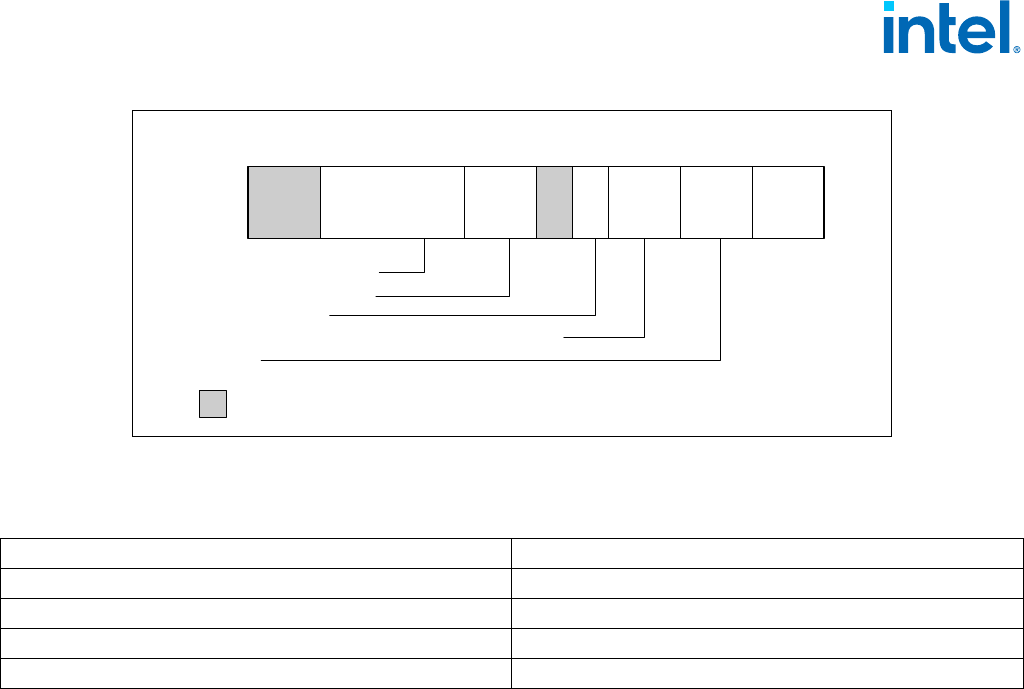
Document Number: 319433-052 1-32
FUTURE INTEL® ARCHITECTURE INSTRUCTION EXTENSIONS AND FEATURES
NOTE
See "Caching Translation Information" in Chapter 4, “Paging,” in the Intel
®
64 and IA-32 Architec-
tures Software Developer’s Manual, Volume 3A, and Chapter 20 in the Intel
®
64 and IA-32 Archi-
tectures Software Developer’s Manual, Volume 1, for information on identifying earlier IA-32
processors.
The Extended Family ID needs to be examined only when the Family ID is 0FH. Integrate the fields into a display
using the following rule:
IF Family_ID
≠ 0FH
THEN Displayed_Family = Family_ID;
ELSE Displayed_Family = Extended_Family_ID + Family_ID;
FI;
(* Show Display_Family as HEX field. *)
The Extended Model ID needs to be examined only when the Family ID is 06H or 0FH. Integrate the field into a
display using the following rule:
IF (Family_ID = 06H or Family_ID = 0FH)
THEN Displayed_Model = (Extended_Model_ID << 4) + Model_ID;
(* Right justify and zero-extend 4-bit field; display Model_ID as HEX field.*)
ELSE Displayed_Model = Model_ID;
FI;
(* Show Display_Model as HEX field. *)
INPUT EAX = 01H: Returns Additional Information in EBX
When CPUID executes with EAX set to 01H, additional information is returned to the EBX register:
Figure 1-1. Version Information Returned by CPUID in EAX
Table 1-4. Processor Type Field
Type Encoding
Original OEM Processor 00B
Intel OverDrive
®
Processor 01B
Dual processor (not applicable to Intel486 processors) 10B
Intel reserved 11B
Processor Type
034781112131415161920272831
EAX
Family (0FH for the Pentium 4 Processor Family)
Model
Extended
Family ID
Extended
Model ID
Family
ID
Model
Stepping
ID
Extended Family ID (0)
Extended Model ID (0)
Reserved

Document Number: 319433-052 1-33
FUTURE INTEL® ARCHITECTURE INSTRUCTION EXTENSIONS AND FEATURES
• Brand index (low byte of EBX) — this number provides an entry into a brand string table that contains brand
strings for IA-32 processors. More information about this field is provided later in this section.
• CLFLUSH instruction cache line size (second byte of EBX) — this number indicates the size of the cache line
flushed with CLFLUSH instruction in 8-byte increments. This field was introduced in the Pentium 4 processor.
• Local APIC ID (high byte of EBX) — this number is the 8-bit ID that is assigned to the local APIC on the
processor during power up. This field was introduced in the Pentium 4 processor.
INPUT EAX = 01H: Returns Feature Information in ECX and EDX
When CPUID executes with EAX set to 01H, feature information is returned in ECX and EDX.
• Figure 1-2 and Table 1-5 show encodings for ECX.
• Figure 1-3 and Table 1-6 show encodings for EDX.
For all feature flags, a 1 indicates that the feature is supported. Use Intel to properly interpret feature flags.
NOTE
Software must confirm that a processor feature is present using feature flags returned by CPUID
prior to using the feature. Software should not depend on future offerings retaining all features.
Figure 1-2. Feature Information Returned in the ECX Register
CNXT-ID — L1 Context ID
012345678910111213141516171819202122232425262728293031
ECX
TM2 — Thermal Monitor 2
EST — Enhanced Intel SpeedStep® Technology
DS-CPL — CPL Qualified Debug Store
MONITOR — MONITOR/MWAIT
PCLMULQDQ — Carryless Multiplication
Reserved
CMPXCHG16B
SMX — Safer Mode Extensions
xTPR Update Control
SSSE3 — SSSE3 Extensions
PDCM — Perf/Debug Capability MSR
VMX — Virtual Machine Extensions
SSE4_1 — SSE4.1
OSXSAVE
SSE4_2 — SSE4.2
DCA — Direct Cache Access
x2APIC
POPCNT
XSAVE
AVX
AES
FMA — Fused Multiply Add
SSE3 — SSE3 Extensions
PCID — Process-context Identifiers
0
DTES64 — 64-bit DS Area
MOVBE
TSC-Deadline
F16C
RDRAND
SDBG

Document Number: 319433-052 1-34
FUTURE INTEL® ARCHITECTURE INSTRUCTION EXTENSIONS AND FEATURES
Table 1-5. Feature Information Returned in the ECX Register
Bit # Mnemonic Description
0 SSE3 Intel
®
Streaming SIMD Extensions 3 (Intel
®
SSE3). A value of 1 indicates the processor supports this
technology.
1 PCLMULQDQ A value of 1 indicates the processor supports the PCLMULQDQ instruction.
2DTES6464-bit DS Area. A value of 1 indicates the processor supports DS area using 64-bit layout.
3 MONITOR MONITOR/MWAIT. A value of 1 indicates the processor supports this feature.
4 DS-CPL CPL Qualified Debug Store. A value of 1 indicates the processor supports the extensions to the
Debug Store feature to allow for branch message storage qualified by CPL.
5VMXVirtual Machine Extensions. A value of 1 indicates that the processor supports this technology.
6SMXSafer Mode Extensions. A value of 1 indicates that the processor supports this technology. See
Chapter 7, “Safer Mode Extensions Reference.”
7 EST Enhanced Intel SpeedStep
®
Technology. A value of 1 indicates that the processor supports this
technology.
8 TM2 Thermal Monitor 2. A value of 1 indicates whether the processor supports this technology.
9 SSSE3 A value of 1 indicates the presence of the Supplemental Streaming SIMD Extensions 3 (SSSE3). A
value of 0 indicates the instruction extensions are not present in the processor.
10 CNXT-ID L1 Context ID. A value of 1 indicates the L1 data cache mode can be set to either adaptive mode or
shared mode. A value of 0 indicates this feature is not supported. See definition of the
IA32_MISC_ENABLE MSR Bit 24 (L1 Data Cache Context Mode) for details.
11 SDBG A value of 1 indicates the processor supports IA32_DEBUG_INTERFACE MSR for silicon debug.
12 FMA A value of 1 indicates the processor supports FMA extensions using YMM state.
13 CMPXCHG16B CMPXCHG16B Available. A value of 1 indicates that the feature is available.
14 xTPR Update
Control
xTPR Update Control. A value of 1 indicates that the processor supports changing
IA32_MISC_ENABLES[bit 23].
15 PDCM Perfmon and Debug Capability. A value of 1 indicates the processor supports the performance and
debug feature indication MSR IA32_PERF_CAPABILITIES.
16 Reserved Reserved.
17 PCID Process-context identifiers. A value of 1 indicates that the processor supports PCIDs and that
software may set CR4.PCIDE to 1.
18 DCA A value of 1 indicates the processor supports the ability to prefetch data from a memory mapped
device.
19 SSE4.1 A value of 1 indicates that the processor supports SSE4.1.
20 SSE4.2 A value of 1 indicates that the processor supports SSE4.2.
21 x2APIC A value of 1 indicates that the processor supports x2APIC feature.
22 MOVBE A value of 1 indicates that the processor supports MOVBE instruction.
23 POPCNT A value of 1 indicates that the processor supports the POPCNT instruction.
24 TSC-Deadline A value of 1 indicates that the processor’s local APIC timer supports one-shot operation using a TSC
deadline value.
25 AES A value of 1 indicates that the processor supports the AESNI instruction extensions.
26 XSAVE A value of 1 indicates that the processor supports the XSAVE/XRSTOR processor extended states
feature, the XSETBV/XGETBV instructions, and XCR0.
27 OSXSAVE A value of 1 indicates that the OS has set CR4.OSXSAVE[bit 18] to enable XSETBV/XGETBV
instructions to access XCR0 and to support processor extended state management using
XSAVE/XRSTOR.
28 AVX A value of 1 indicates that processor supports AVX instructions operating on 256-bit YMM state, and
three-operand encoding of 256-bit and 128-bit SIMD instructions.

Document Number: 319433-052 1-35
FUTURE INTEL® ARCHITECTURE INSTRUCTION EXTENSIONS AND FEATURES
29 F16C A value of 1 indicates that processor supports 16-bit floating-point conversion instructions.
30 RDRAND A value of 1 indicates that processor supports RDRAND instruction.
31 Not Used Always return 0.
Figure 1-3. Feature Information Returned in the EDX Register
Table 1-6. More on Feature Information Returned in the EDX Register
Bit # Mnemonic Description
0 FPU Floating-point Unit On-Chip. The processor contains an x87 FPU.
1 VME Virtual 8086 Mode Enhancements. Virtual 8086 mode enhancements, including CR4.VME for controlling
the feature, CR4.PVI for protected mode virtual interrupts, software interrupt indirection, expansion of the
TSS with the software indirection bitmap, and EFLAGS.VIF and EFLAGS.VIP flags.
2 DE Debugging Extensions. Support for I/O breakpoints, including CR4.DE for controlling the feature, and
optional trapping of accesses to DR4 and DR5.
Table 1-5. Feature Information Returned in the ECX Register (Continued)
Bit # Mnemonic Description
PBE–Pend. Brk. EN.
012345678910111213141516171819202122232425262728293031
EDX
TM–Therm. Monitor
HTT–Multi-threading
SS–Self Snoop
SSE2–SSE2 Extensions
SSE–SSE Extensions
FXSR–FXSAVE/FXRSTOR
MMX–MMX Technology
ACPI–Thermal Monitor and Clock Ctrl
DS–Debug Store
CLFSH–CFLUSH instruction
PSN–Processor Serial Number
PSE-36 – Page Size Extension
PAT–Page Attribute Table
CMOV–Conditional Move/Compare Instruction
MCA–Machine Check Architecture
PGE–PTE Global Bit
MTRR–Memory Type Range Registers
SEP–SYSENTER and SYSEXIT
APIC–APIC on Chip
CX8–CMPXCHG8B Inst.
MCE–Machine Check Exception
PAE–Physical Address Extensions
MSR–RDMSR and WRMSR Support
TSC–Time Stamp Counter
PSE–Page Size Extensions
DE–Debugging Extensions
VME–Virtual-8086 Mode Enhancement
FPU–x87 FPU on Chip
Reserved

Document Number: 319433-052 1-36
FUTURE INTEL® ARCHITECTURE INSTRUCTION EXTENSIONS AND FEATURES
3 PSE Page Size Extension. Large pages of size 4 MByte are supported, including CR4.PSE for controlling the
feature, the defined dirty bit in PDE (Page Directory Entries), optional reserved bit trapping in CR3, PDEs,
and PTEs.
4 TSC Time Stamp Counter. The RDTSC instruction is supported, including CR4.TSD for controlling privilege.
5 MSR Model Specific Registers RDMSR and WRMSR Instructions. The RDMSR and WRMSR instructions are
supported. Some of the MSRs are implementation dependent.
6 PAE Physical Address Extension. Physical addresses greater than 32 bits are supported: extended page table
entry formats, an extra level in the page translation tables is defined, 2-MByte pages are supported instead
of 4 Mbyte pages if PAE bit is 1. The actual number of address bits beyond 32 is not defined, and is
implementation specific.
7 MCE Machine Check Exception. Exception 18 is defined for Machine Checks, including CR4.MCE for controlling
the feature. This feature does not define the model-specific implementations of machine-check error
logging, reporting, and processor shutdowns. Machine Check exception handlers may have to depend on
processor version to do model specific processing of the exception, or test for the presence of the Machine
Check feature.
8 CX8 CMPXCHG8B Instruction. The compare-and-exchange 8 bytes (64 bits) instruction is supported (implicitly
locked and atomic).
9 APIC APIC On-Chip. The processor contains an Advanced Programmable Interrupt Controller (APIC), responding
to memory mapped commands in the physical address range FFFE0000H to FFFE0FFFH (by default - some
processors permit the APIC to be relocated).
10 Reserved Reserved.
11 SEP SYSENTER and SYSEXIT Instructions. The SYSENTER and SYSEXIT and associated MSRs are supported.
12 MTRR Memory Type Range Registers. MTRRs are supported. The MTRRcap MSR contains feature bits that
describe what memory types are supported, how many variable MTRRs are supported, and whether fixed
MTRRs are supported.
13 PGE Page Global Bit. The global bit is supported in paging-structure entries that map a page, indicating TLB
entries that are common to different processes and need not be flushed. The CR4.PGE bit controls this
feature.
14 MCA Machine Check Architecture. The Machine Check Architecture, which provides a compatible mechanism for
error reporting in P6 family, Pentium 4, Intel Xeon processors, and future processors, is supported. The
MCG_CAP MSR contains feature bits describing how many banks of error reporting MSRs are supported.
15 CMOV Conditional Move Instructions. The conditional move instruction CMOV is supported. In addition, if x87
FPU is present as indicated by the CPUID.FPU feature bit, then the FCOMI and FCMOV instructions are
supported
16 PAT Page Attribute Table. Page Attribute Table is supported. This feature augments the Memory Type Range
Registers (MTRRs), allowing an operating system to specify attributes of memory accessed through a linear
address on a 4KB granularity.
17 PSE-36 36-Bit Page Size Extension. 4-MByte pages addressing physical memory beyond 4 GBytes are supported
with 32-bit paging. This feature indicates that upper bits of the physical address of a 4-MByte page are
encoded in bits 20:13 of the page-directory entry. Such physical addresses are limited by MAXPHYADDR
and may be up to 40 bits in size.
18 PSN Processor Serial Number. The processor supports the 96-bit processor identification number feature and
the feature is enabled.
19 CLFSH CLFLUSH Instruction. CLFLUSH Instruction is supported.
20 Reserved Reserved.
Table 1-6. More on Feature Information Returned in the EDX Register (Continued)
Bit # Mnemonic Description

Document Number: 319433-052 1-37
FUTURE INTEL® ARCHITECTURE INSTRUCTION EXTENSIONS AND FEATURES
INPUT EAX = 02H: Cache and TLB Information Returned in EAX, EBX, ECX, EDX
When CPUID executes with EAX set to 02H, the processor returns information about the processor’s internal caches
and TLBs in the EAX, EBX, ECX, and EDX registers.
The encoding is as follows:
• The least-significant byte in register EAX (register AL) indicates the number of times the CPUID instruction
must be executed with an input value of 02H to get a complete description of the processor’s caches and TLBs.
The first member of the family of Pentium 4 processors will return a 01H.
• The most significant bit (bit 31) of each register indicates whether the register contains valid information (set
to 0) or is reserved (set to 1).
• If a register contains valid information, the information is contained in 1 byte descriptors. Table 1-7 shows the
encoding of these descriptors. Note that the order of descriptors in the EAX, EBX, ECX, and EDX registers is not
defined; that is, specific bytes are not designated to contain descriptors for specific cache or TLB types. The
descriptors may appear in any order.
21 DS Debug Store. The processor supports the ability to write debug information into a memory resident buffer.
This feature is used by the branch trace store (BTS) and precise event-based sampling (PEBS) facilities (see
Chapter 24, “Introduction to Virtual-Machine Extensions,” in the Intel
®
64 and IA-32 Architectures
Software Developer’s Manual, Volume 3C).
22 ACPI Thermal Monitor and Software Controlled Clock Facilities. The processor implements internal MSRs that
allow processor temperature to be monitored and processor performance to be modulated in predefined
duty cycles under software control.
23 MMX Intel MMX Technology. The processor supports the Intel MMX technology.
24 FXSR FXSAVE and FXRSTOR Instructions. The FXSAVE and FXRSTOR instructions are supported for fast save
and restore of the floating-point context. Presence of this bit also indicates that CR4.OSFXSR is available
for an operating system to indicate that it supports the FXSAVE and FXRSTOR instructions.
25 SSE SSE. The processor supports the SSE extensions.
26 SSE2 SSE2. The processor supports the SSE2 extensions.
27 SS Self Snoop. The processor supports the management of conflicting memory types by performing a snoop
of its own cache structure for transactions issued to the bus.
28 HTT Max APIC IDs reserved field is Valid. A value of 0 for HTT indicates there is only a single logical processor
in the package and software should assume only a single APIC ID is reserved. A value of 1 for HTT indicates
the value in CPUID.1.EBX[23:16] (the Maximum number of addressable IDs for logical processors in this
package) is valid for the package.
29 TM Thermal Monitor. The processor implements the thermal monitor automatic thermal control circuitry (TCC).
30 Reserved Reserved.
31 PBE Pending Break Enable. The processor supports the use of the FERR#/PBE# pin when the processor is in
the stop-clock state (STPCLK# is asserted) to signal the processor that an interrupt is pending and that the
processor should return to normal operation to handle the interrupt. Bit 10 (PBE enable) in the
IA32_MISC_ENABLE MSR enables this capability.
Table 1-7. Encoding of CPUID Leaf 2 Descriptors
Descriptor
Value
Type Cache or TLB Description
00H General Null descriptor, this byte contains no information.
01H TLB Instruction TLB: 4 KByte pages, 4-way set associative, 32 entries.
02H TLB Instruction TLB: 4 MByte pages, fully associative, 2 entries.
03H TLB Data TLB: 4 KByte pages, 4-way set associative, 64 entries.
Table 1-6. More on Feature Information Returned in the EDX Register (Continued)
Bit # Mnemonic Description

Document Number: 319433-052 1-38
FUTURE INTEL® ARCHITECTURE INSTRUCTION EXTENSIONS AND FEATURES
04H TLB Data TLB: 4 MByte pages, 4-way set associative, 8 entries.
05H TLB Data TLB1: 4 MByte pages, 4-way set associative, 32 entries.
06H Cache 1st-level instruction cache: 8 KBytes, 4-way set associative, 32 byte line size.
08H Cache 1st-level instruction cache: 16 KBytes, 4-way set associative, 32 byte line size.
09H Cache 1st-level instruction cache: 32KBytes, 4-way set associative, 64 byte line size.
0AH Cache 1st-level data cache: 8 KBytes, 2-way set associative, 32 byte line size.
0BH TLB Instruction TLB: 4 MByte pages, 4-way set associative, 4 entries.
0CH Cache 1st-level data cache: 16 KBytes, 4-way set associative, 32 byte line size.
0DH Cache 1st-level data cache: 16 KBytes, 4-way set associative, 64 byte line size.
0EH Cache 1st-level data cache: 24 KBytes, 6-way set associative, 64 byte line size.
1DH Cache 2nd-level cache: 128 KBytes, 2-way set associative, 64 byte line size.
21H Cache 2nd-level cache: 256 KBytes, 8-way set associative, 64 byte line size.
22H Cache 3rd-level cache: 512 KBytes, 4-way set associative, 64 byte line size, 2 lines per sector.
23H Cache 3rd-level cache: 1 MBytes, 8-way set associative, 64 byte line size, 2 lines per sector.
24H Cache 2nd-level cache: 1 MBytes, 16-way set associative, 64 byte line size.
25H Cache 3rd-level cache: 2 MBytes, 8-way set associative, 64 byte line size, 2 lines per sector.
29H Cache 3rd-level cache: 4 MBytes, 8-way set associative, 64 byte line size, 2 lines per sector.
2CH Cache 1st-level data cache: 32 KBytes, 8-way set associative, 64 byte line size.
30H Cache 1st-level instruction cache: 32 KBytes, 8-way set associative, 64 byte line size.
40H Cache No 2nd-level cache or, if processor contains a valid 2nd-level cache, no 3rd-level cache.
41H Cache 2nd-level cache: 128 KBytes, 4-way set associative, 32 byte line size.
42H Cache 2nd-level cache: 256 KBytes, 4-way set associative, 32 byte line size.
43H Cache 2nd-level cache: 512 KBytes, 4-way set associative, 32 byte line size.
44H Cache 2nd-level cache: 1 MByte, 4-way set associative, 32 byte line size.
45H Cache 2nd-level cache: 2 MByte, 4-way set associative, 32 byte line size.
46H Cache 3rd-level cache: 4 MByte, 4-way set associative, 64 byte line size.
47H Cache 3rd-level cache: 8 MByte, 8-way set associative, 64 byte line size.
48H Cache 2nd-level cache: 3MByte, 12-way set associative, 64 byte line size.
49H Cache 3rd-level cache: 4MB, 16-way set associative, 64-byte line size (Intel Xeon processor MP, Family 0FH,
Model 06H);
2nd-level cache: 4 MByte, 16-way set associative, 64 byte line size.
4AH Cache 3rd-level cache: 6MByte, 12-way set associative, 64 byte line size.
4BH Cache 3rd-level cache: 8MByte, 16-way set associative, 64 byte line size.
4CH Cache 3rd-level cache: 12MByte, 12-way set associative, 64 byte line size.
4DH Cache 3rd-level cache: 16MByte, 16-way set associative, 64 byte line size.
4EH Cache 2nd-level cache: 6MByte, 24-way set associative, 64 byte line size.
4FH TLB Instruction TLB: 4 KByte pages, 32 entries.
50H TLB Instruction TLB: 4 KByte and 2-MByte or 4-MByte pages, 64 entries.
51H TLB Instruction TLB: 4 KByte and 2-MByte or 4-MByte pages, 128 entries.
52H TLB Instruction TLB: 4 KByte and 2-MByte or 4-MByte pages, 256 entries.
55H TLB Instruction TLB: 2-MByte or 4-MByte pages, fully associative, 7 entries.
Table 1-7. Encoding of CPUID Leaf 2 Descriptors (Continued)
Descriptor
Value
Type Cache or TLB Description

Document Number: 319433-052 1-39
FUTURE INTEL® ARCHITECTURE INSTRUCTION EXTENSIONS AND FEATURES
56H TLB Data TLB0: 4 MByte pages, 4-way set associative, 16 entries.
57H TLB Data TLB0: 4 KByte pages, 4-way associative, 16 entries.
59H TLB Data TLB0: 4 KByte pages, fully associative, 16 entries.
5AH TLB Data TLB0: 2 MByte or 4 MByte pages, 4-way set associative, 32 entries.
5BH TLB Data TLB: 4 KByte and 4 MByte pages, 64 entries.
5CH TLB Data TLB: 4 KByte and 4 MByte pages,128 entries.
5DH TLB Data TLB: 4 KByte and 4 MByte pages,256 entries.
60H Cache 1st-level data cache: 16 KByte, 8-way set associative, 64 byte line size.
61H TLB Instruction TLB: 4 KByte pages, fully associative, 48 entries.
63H TLB Data TLB: 2 MByte or 4 MByte pages, 4-way set associative, 32 entries and a separate array with 1
GByte pages, 4-way set associative, 4 entries.
64H TLB Data TLB: 4 KByte pages, 4-way set associative, 512 entries.
66H Cache 1st-level data cache: 8 KByte, 4-way set associative, 64 byte line size.
67H Cache 1st-level data cache: 16 KByte, 4-way set associative, 64 byte line size.
68H Cache 1st-level data cache: 32 KByte, 4-way set associative, 64 byte line size.
6AH Cache uTLB: 4 KByte pages, 8-way set associative, 64 entries.
6BH Cache DTLB: 4 KByte pages, 8-way set associative, 256 entries.
6CH Cache DTLB: 2M/4M pages, 8-way set associative, 128 entries.
6DH Cache DTLB: 1 GByte pages, fully associative, 16 entries.
70H Cache Trace cache: 12 K-μop, 8-way set associative.
71H Cache Trace cache: 16 K-μop, 8-way set associative.
72H Cache Trace cache: 32 K-μop, 8-way set associative.
76H TLB Instruction TLB: 2M/4M pages, fully associative, 8 entries.
78H Cache 2nd-level cache: 1 MByte, 4-way set associative, 64byte line size.
79H Cache 2nd-level cache: 128 KByte, 8-way set associative, 64 byte line size, 2 lines per sector.
7AH Cache 2nd-level cache: 256 KByte, 8-way set associative, 64 byte line size, 2 lines per sector.
7BH Cache 2nd-level cache: 512 KByte, 8-way set associative, 64 byte line size, 2 lines per sector.
7CH Cache 2nd-level cache: 1 MByte, 8-way set associative, 64 byte line size, 2 lines per sector.
7DH Cache 2nd-level cache: 2 MByte, 8-way set associative, 64byte line size.
7FH Cache 2nd-level cache: 512 KByte, 2-way set associative, 64-byte line size.
80H Cache 2nd-level cache: 512 KByte, 8-way set associative, 64-byte line size.
82H Cache 2nd-level cache: 256 KByte, 8-way set associative, 32 byte line size.
83H Cache 2nd-level cache: 512 KByte, 8-way set associative, 32 byte line size.
84H Cache 2nd-level cache: 1 MByte, 8-way set associative, 32 byte line size.
85H Cache 2nd-level cache: 2 MByte, 8-way set associative, 32 byte line size.
86H Cache 2nd-level cache: 512 KByte, 4-way set associative, 64 byte line size.
87H Cache 2nd-level cache: 1 MByte, 8-way set associative, 64 byte line size.
A0H DTLB DTLB: 4k pages, fully associative, 32 entries.
B0H TLB Instruction TLB: 4 KByte pages, 4-way set associative, 128 entries.
B1H TLB Instruction TLB: 2M pages, 4-way, 8 entries or 4M pages, 4-way, 4 entries.
B2H TLB Instruction TLB: 4KByte pages, 4-way set associative, 64 entries.
Table 1-7. Encoding of CPUID Leaf 2 Descriptors (Continued)
Descriptor
Value
Type Cache or TLB Description

Document Number: 319433-052 1-40
FUTURE INTEL® ARCHITECTURE INSTRUCTION EXTENSIONS AND FEATURES
Example 1-1. Example of Cache and TLB Interpretation
The first member of the family of Pentium 4 processors returns the following information about caches and TLBs
when the CPUID executes with an input value of 2:
EAX 66 5B 50 01H
EBX 0H
ECX 0H
EDX 00 7A 70 00H
Which means:
B3H TLB Data TLB: 4 KByte pages, 4-way set associative, 128 entries.
B4H TLB Data TLB1: 4 KByte pages, 4-way associative, 256 entries.
B5H TLB Instruction TLB: 4KByte pages, 8-way set associative, 64 entries.
B6H TLB Instruction TLB: 4KByte pages, 8-way set associative, 128 entries.
BAH TLB Data TLB1: 4 KByte pages, 4-way associative, 64 entries.
C0H TLB Data TLB: 4 KByte and 4 MByte pages, 4-way associative, 8 entries.
C1H STLB Shared 2nd-Level TLB: 4 KByte/2MByte pages, 8-way associative, 1024 entries.
C2H DTLB DTLB: 4 KByte/2 MByte pages, 4-way associative, 16 entries.
C3H STLB Shared 2nd-Level TLB: 4 KByte /2 MByte pages, 6-way associative, 1536 entries. Also 1GBbyte pages,
4-way, 16 entries.
C4H DTLB DTLB: 2M/4M Byte pages, 4-way associative, 32 entries.
CAH STLB Shared 2nd-Level TLB: 4 KByte pages, 4-way associative, 512 entries.
D0H Cache 3rd-level cache: 512 KByte, 4-way set associative, 64 byte line size.
D1H Cache 3rd-level cache: 1 MByte, 4-way set associative, 64 byte line size.
D2H Cache 3rd-level cache: 2 MByte, 4-way set associative, 64 byte line size.
D6H Cache 3rd-level cache: 1 MByte, 8-way set associative, 64 byte line size.
D7H Cache 3rd-level cache: 2 MByte, 8-way set associative, 64 byte line size.
D8H Cache 3rd-level cache: 4 MByte, 8-way set associative, 64 byte line size.
DCH Cache 3rd-level cache: 1.5 MByte, 12-way set associative, 64 byte line size.
DDH Cache 3rd-level cache: 3 MByte, 12-way set associative, 64 byte line size.
DEH Cache 3rd-level cache: 6 MByte, 12-way set associative, 64 byte line size.
E2H Cache 3rd-level cache: 2 MByte, 16-way set associative, 64 byte line size.
E3H Cache 3rd-level cache: 4 MByte, 16-way set associative, 64 byte line size.
E4H Cache 3rd-level cache: 8 MByte, 16-way set associative, 64 byte line size.
EAH Cache 3rd-level cache: 12MByte, 24-way set associative, 64 byte line size.
EBH Cache 3rd-level cache: 18MByte, 24-way set associative, 64 byte line size.
ECH Cache 3rd-level cache: 24MByte, 24-way set associative, 64 byte line size.
F0H Prefetch 64-Byte prefetching.
F1H Prefetch 128-Byte prefetching.
FEH General CPUID leaf 2 does not report TLB descriptor information; use CPUID leaf 18H to query TLB and other
address translation parameters.
FFH General CPUID leaf 2 does not report cache descriptor information, use CPUID leaf 4 to query cache parameters.
Table 1-7. Encoding of CPUID Leaf 2 Descriptors (Continued)
Descriptor
Value
Type Cache or TLB Description

Document Number: 319433-052 1-41
FUTURE INTEL® ARCHITECTURE INSTRUCTION EXTENSIONS AND FEATURES
• The least-significant byte (byte 0) of register EAX is set to 01H. This indicates that CPUID needs to be executed
once with an input value of 2 to retrieve complete information about caches and TLBs.
• The most-significant bit of all four registers (EAX, EBX, ECX, and EDX) is set to 0, indicating that each register
contains valid 1-byte descriptors.
• Bytes 1, 2, and 3 of register EAX indicate that the processor has:
— 50H - a 64-entry instruction TLB, for mapping 4-KByte and 2-MByte or 4-MByte pages.
— 5BH - a 64-entry data TLB, for mapping 4-KByte and 4-MByte pages.
— 66H - an 8-KByte 1st level data cache, 4-way set associative, with a 64-Byte cache line size.
• The descriptors in registers EBX and ECX are valid, but contain NULL descriptors.
• Bytes 0, 1, 2, and 3 of register EDX indicate that the processor has:
— 00H - NULL descriptor.
— 70H - Trace cache: 12 K-μop, 8-way set associative.
— 7AH - a 256-KByte 2nd level cache, 8-way set associative, with a sectored, 64-byte cache line size.
— 00H - NULL descriptor.
INPUT EAX = 04H: Returns Deterministic Cache Parameters for Each Level
When CPUID executes with EAX set to 04H and ECX contains an index value, the processor returns encoded data
that describe a set of deterministic cache parameters (for the cache level associated with the input in ECX). Valid
index values start from 0.
Software can enumerate the deterministic cache parameters for each level of the cache hierarchy starting with an
index value of 0, until the parameters report the value associated with the cache type field is 0. The architecturally
defined fields reported by deterministic cache parameters are documented in Table 1-3.
The CPUID leaf 4 also reports data that can be used to derive the topology of processor cores in a physical package.
This information is constant for all valid index values. Software can query the raw data reported by executing
CPUID with EAX=04H and ECX=0H and use it as part of the topology enumeration algorithm described in Chapter
9, “Multiple-Processor Management,” in the Intel
®
64 and IA-32 Architectures Software Developer’s Manual,
Volume 3A.
INPUT EAX = 05H: Returns MONITOR and MWAIT Features
When CPUID executes with EAX set to 05H, the processor returns information about features available to
MONITOR/MWAIT instructions. The MONITOR instruction is used for address-range monitoring in conjunction with
MWAIT instruction. The MWAIT instruction optionally provides additional extensions for advanced power manage-
ment. See Table 1-3.
INPUT EAX = 06H: Returns Thermal and Power Management Features
When CPUID executes with EAX set to 06H, the processor returns information about thermal and power manage-
ment features. See Table 1-3.
INPUT EAX = 07H: Returns Structured Extended Feature Enumeration Information
When CPUID executes with EAX set to 07H and ECX = 0H, the processor returns information about the maximum
number of sub-leaves that contain extended feature flags. See Table 1-3.
When CPUID executes with EAX set to 07H and ECX = n (n
≥ 1 and less than the number of non-zero bits in
CPUID.(EAX=07H, ECX= 0H).EAX), the processor returns information about extended feature flags. See Table 1-3.
In sub-leaf 0, only EAX has the number of sub-leaves. In sub-leaf 0, EBX, ECX & EDX all contain extended feature
flags.
INPUT EAX = 09H: Returns Direct Cache Access Information
When CPUID executes with EAX set to 09H, the processor returns information about Direct Cache Access capabili-
ties. See Table 1-3.

Document Number: 319433-052 1-42
FUTURE INTEL® ARCHITECTURE INSTRUCTION EXTENSIONS AND FEATURES
INPUT EAX = 0AH: Returns Architectural Performance Monitoring Features
When CPUID executes with EAX set to 0AH, the processor returns information about support for architectural
performance monitoring capabilities. Architectural performance monitoring is supported if the version ID (see
Table 1-3) is greater than Pn 0. See Table 1-3.
For each version of architectural performance monitoring capability, software must enumerate this leaf to discover
the programming facilities and the architectural performance events available in the processor. The details are
described in Chapter 18, “Debug, Branch Profile, TSC, and Intel
®
Resource Director Technology (Intel
®
RDT)
Features,” in the Intel
®
64 and IA-32 Architectures Software Developer’s Manual, Volume 3A.
INPUT EAX = 0BH: Returns Extended Topology Information
CPUID leaf 1FH is a preferred superset to leaf 0BH. Intel recommends first checking for the existence of Leaf 1FH
before using leaf 0BH.
When CPUID executes with EAX set to 0BH, the processor returns information about extended topology enumera-
tion data. Software must detect the presence of CPUID leaf 0BH by verifying (a) the highest leaf index supported
by CPUID is >= 0BH, and (b) CPUID.0BH:EBX[15:0] reports a non-zero value. See Table 1-3.
INPUT EAX = 0DH: Returns Processor Extended States Enumeration Information
When CPUID executes with EAX set to 0DH and ECX = 0H, the processor returns information about the bit-vector
representation of all processor state extensions that are supported in the processor and storage size requirements
of the XSAVE/XRSTOR area. See Table 1-3.
When CPUID executes with EAX set to 0DH and ECX = n (n > 1, and is a valid sub-leaf index), the processor returns
information about the size and offset of each processor extended state save area within the XSAVE/XRSTOR area.
See Table 1-3. Software can use the forward-extendable technique depicted below to query the valid sub-leaves
and obtain size and offset information for each processor extended state save area:
For i = 2 to 62 // sub-leaf 1 is reserved
IF (CPUID.(EAX=0DH, ECX=0):VECTOR[i] = 1 ) // VECTOR is the 64-bit value of EDX:EAX
Execute CPUID.(EAX=0DH, ECX = i) to examine size and offset for sub-leaf i;
FI;
INPUT EAX = 0FH: Returns Intel Resource Director Technology (Intel RDT) Monitoring Enumeration Information
When CPUID executes with EAX set to 0FH and ECX = 0, the processor returns information about the bit-vector
representation of QoS monitoring resource types that are supported in the processor and maximum range of RMID
values the processor can use to monitor of any supported resource types. Each bit, starting from bit 1, corresponds
to a specific resource type if the bit is set. The bit position corresponds to the sub-leaf index (or ResID) that soft-
ware must use to query QoS monitoring capability available for that type. See Table 1-3.
When CPUID executes with EAX set to 0FH and ECX = n (n >= 1, and is a valid ResID), the processor returns infor-
mation software can use to program IA32_PQR_ASSOC, IA32_QM_EVTSEL MSRs before reading QoS data from the
IA32_QM_CTR MSR.
INPUT EAX = 10H: Returns Intel Resource Director Technology (Intel RDT) Allocation Enumeration Information
When CPUID executes with EAX set to 10H and ECX = 0, the processor returns information about the bit-vector
representation of QoS Enforcement resource types that are supported in the processor. Each bit, starting from bit
1, corresponds to a specific resource type if the bit is set. The bit position corresponds to the sub-leaf index (or
ResID) that software must use to query QoS enforcement capability available for that type. See Table 1-3.
When CPUID executes with EAX set to 10H and ECX = n (n >= 1, and is a valid ResID), the processor returns infor-
mation about available classes of service and range of QoS mask MSRs that software can use to configure each
class of services using capability bit masks in the QoS Mask registers, IA32_resourceType_Mask_n.
INPUT EAX = 12H: Returns Intel SGX Enumeration Information
When CPUID executes with EAX set to 12H and ECX = 0H, the processor returns information about Intel SGX capa-
bilities. See Table 1-3.

Document Number: 319433-052 1-43
FUTURE INTEL® ARCHITECTURE INSTRUCTION EXTENSIONS AND FEATURES
When CPUID executes with EAX set to 12H and ECX = 1H, the processor returns information about Intel SGX attri-
butes. See Table 1-3.
When CPUID executes with EAX set to 12H and ECX = n (n > 1), the processor returns information about Intel SGX
Enclave Page Cache. See Table 1-3.
INPUT EAX = 14H: Returns Intel Processor Trace Enumeration Information
When CPUID executes with EAX set to 14H and ECX = 0H, the processor returns information about Intel Processor
Trace extensions. See Table 1-3.
When CPUID executes with EAX set to 14H and ECX = n (n > 0 and less than the number of non-zero bits in
CPUID.(EAX=14H, ECX= 0H).EAX), the processor returns information about packet generation in Intel Processor
Trace. See Table 1-3.
INPUT EAX = 15H: Returns Time Stamp Counter and Nominal Core Crystal Clock Information
When CPUID executes with EAX set to 15H and ECX = 0H, the processor returns information about Time Stamp
Counter and Core Crystal Clock. See Table 1-3.
INPUT EAX = 16H: Returns Processor Frequency Information
When CPUID executes with EAX set to 16H, the processor returns information about Processor Frequency Informa-
tion. See Table 1-3.
INPUT EAX = 17H: Returns System-On-Chip Information
When CPUID executes with EAX set to 17H, the processor returns information about the System-On-Chip Vendor
Attribute Enumeration. See Table 1-3.
INPUT EAX = 18H: Returns Deterministic Address Translation Parameters Information
When CPUID executes with EAX set to 18H, the processor returns information about the Deterministic Address
Translation Parameters. See Table 1-3.
INPUT EAX = 19H: Returns Key Locker Information
When CPUID executes with EAX set to 19H, the processor returns information about Key Locker. See Table 1-3.
INPUT EAX = 1AH: Returns Hybrid Information
When CPUID executes with EAX set to 1AH, the processor returns information about hybrid capabilities. See Table
1-3.
INPUT EAX = 1BH: Returns PCONFIG Information
When CPUID executes with EAX set to 1BH, the processor returns information about PCONFIG capabilities. This
information is enumerated in sub-leaves selected by the value of ECX (starting with 0).
Each sub-leaf of CPUID function 1BH enumerates its sub-leaf type in EAX. If a sub-leaf type is 0, the sub-leaf is
invalid and zero is returned in EBX, ECX, and EDX. In this case, all subsequent sub-leaves (selected by larger input
values of ECX) are also invalid.
The only valid sub-leaf type currently defined is 1, indicating that the sub-leaf enumerates target identifiers for the
PCONFIG instruction. Any non-zero value returned in EBX, ECX, or EDX indicates a valid target identifier of the
PCONFIG instruction (any value of zero should be ignored). Currently, TME-MK and TSE are the only defined
targets. TME-MK is indicated by identifier 1, and TSE is indicated by identifier 2. An identifier of 0 indicates an
invalid target. If TME-MK is a supported target, the MKTME_KEY_PROGRAM leaf of PCONFIG is available. If TSE is
a supported target, the TSE_KEY_PROGRAM and the TSE_KEY_PROGRAM_WRAPPED leaves of PCONFIG are avail-
able. See the “PCONFIG-Platform Configuration” instruction in Chapter 4 of the Intel® 64 and IA 32 Architectures
Software Developer's Manual, Volume 2B, for more information.

Document Number: 319433-052 1-44
FUTURE INTEL® ARCHITECTURE INSTRUCTION EXTENSIONS AND FEATURES
INPUT EAX = 1CH: Returns Last Branch Record Information
When CPUID executes with EAX set to 1CH, the processor returns information about LBRs (the architectural
feature). See Table 1-3.
INPUT EAX = 1DH: Returns Tile Information
When CPUID executes with EAX set to 1DH and ECX = 0H, the processor returns information about tile
architecture. See Table 1-3.
When CPUID executes with EAX set to 1DH and ECX = 1H, the processor returns information about tile palette 1.
See Table 1-3.
INPUT EAX = 1EH: Returns TMUL Information
When CPUID executes with EAX set to 1EH and ECX = 0H, the processor returns information about TMUL
capabilities. See Table 1-3.
INPUT EAX = 1FH: Returns V2 Extended Topology Information
When CPUID executes with EAX set to 1FH, the processor returns information about extended topology enumera-
tion data. Software must detect the presence of CPUID leaf 1FH by verifying (a) the highest leaf index supported
by CPUID is >= 1FH, and (b) CPUID.1FH:EBX[15:0] reports a non-zero value. See Table 1-3.
INPUT EAX = 20H: Returns Processor History Reset Information
When CPUID executes with EAX set to 20H, the processor returns information about processor history reset. See
Table 1-3.
INPUT EAX = 23H: Returns Architectural Performance Monitoring Extended Information
When CPUID executes with EAX set to 23H, the processor returns architectural performance monitoring extended
information. See Table 1-3.
INPUT EAX = 24H: Returns Intel AVX10 Converged Vector ISA Information
When CPUID executes with EAX set to 24H, the processor returns Intel AVX10 converged vector ISA information.
See Table 1-3.
METHODS FOR RETURNING BRANDING INFORMATION
Use the following techniques to access branding information:
1. Processor brand string method; this method also returns the processor’s maximum operating frequency
2. Processor brand index; this method uses a software supplied brand string table.
These two methods are discussed in the following sections. For methods that are available in early processors, see
Section: “Identification of Earlier IA-32 Processors” in Chapter 20 of the Intel
®
64 and IA-32 Architectures Soft-
ware Developer’s Manual, Volume 1.
The Processor Brand String Method
Figure 1-4 describes the algorithm used for detection of the brand string. Processor brand identification software
should execute this algorithm on all Intel 64 and IA-32 processors.
This method (introduced with Pentium 4 processors) returns an ASCII brand identification string and the maximum
operating frequency of the processor to the EAX, EBX, ECX, and EDX registers.

Document Number: 319433-052 1-45
FUTURE INTEL® ARCHITECTURE INSTRUCTION EXTENSIONS AND FEATURES
How Brand Strings Work
To use the brand string method, execute CPUID with EAX input of 8000002H through 80000004H. For each input
value, CPUID returns 16 ASCII characters using EAX, EBX, ECX, and EDX. The returned string will be NULL-termi-
nated.
Table 1-8 shows the brand string that is returned by the first processor in the Pentium 4 processor family.
Figure 1-4. Determination of Support for the Processor Brand String
Table 1-8. Processor Brand String Returned with Pentium 4 Processor
EAX Input Value Return Values ASCII Equivalent
80000002H EAX = 20202020H
EBX = 20202020H
ECX = 20202020H
EDX = 6E492020H
“ ”
“”
“”
“nI ”
80000003H EAX = 286C6574H
EBX = 50202952H
ECX = 69746E65H
EDX = 52286D75H
“(let”
“P )R”
“itne”
“R(mu”
80000004H EAX = 20342029H
EBX = 20555043H
ECX = 30303531H
EDX = 007A484DH
“ 4 )”
“ UPC”
“0051”
“\0zHM”
IF (EAX & 0x80000000)
CPUID
IF (EAX Return Value
= 0x80000004)
CPUID
Function
Supported
True =
Extended
EAX Return Value =
Max. Extended CPUID
Function Index
Input: EAX=
0x80000000
Processor Brand
String Not
Supported
False
Processor Brand
String Supported
True

Document Number: 319433-052 1-46
FUTURE INTEL® ARCHITECTURE INSTRUCTION EXTENSIONS AND FEATURES
Extracting the Maximum Processor Frequency from Brand Strings
Figure 1-5 provides an algorithm which software can use to extract the maximum processor operating frequency
from the processor brand string.
NOTE
When a frequency is given in a brand string, it is the maximum qualified frequency of the processor,
not the frequency at which the processor is currently running.
The Processor Brand Index Method
The brand index method (introduced with Pentium
®
III Xeon
®
processors) provides an entry point into a brand
identification table that is maintained in memory by system software and is accessible from system- and user-level
code. In this table, each brand index is associate with an ASCII brand identification string that identifies the official
Intel family and model number of a processor.
When CPUID executes with EAX set to 01H, the processor returns a brand index to the low byte in EBX. Software
can then use this index to locate the brand identification string for the processor in the brand identification table.
The first entry (brand index 0) in this table is reserved, allowing for backward compatibility with processors that do
not support the brand identification feature. Starting with processor signature family ID = 0FH, model = 03H,
brand index method is no longer supported. Use brand string method instead.
Table 1-9 shows brand indices that have identification strings associated with them.
Figure 1-5. Algorithm for Extracting Maximum Processor Frequency
IF Substring Matched
"zHM", or
"zHG", or
"zHT"
True
Determine "Multiplier"
Scan "Brand String" in
Reverse Byte Order
Report Error
False
Scan Digits
Until Blank
Match
Substring
Determine "Freq"
Reverse Digits
To Decimal Value
Max. Qualified
Frequency =
"Freq" x "Multiplier"
"Freq" = X.YZ if
Digits = "ZY.X"
In Reverse Order
If "zHM"
If "zHG"
If "zHT"
Multiplier = 1 x 10
12
Multiplier = 1 x 10
9
Multiplier = 1 x 10
6

Document Number: 319433-052 1-47
FUTURE INTEL® ARCHITECTURE INSTRUCTION EXTENSIONS AND FEATURES
IA-32 Architecture Compatibility
CPUID is not supported in early models of the Intel486 processor or in any IA-32 processor earlier than the
Intel486 processor.
Operation
IA32_BIOS_SIGN_ID MSR := Update with installed microcode revision number;
CASE (EAX) OF
EAX = 0:
EAX := Highest basic function input value understood by CPUID;
EBX := Vendor identification string;
EDX := Vendor identification string;
ECX := Vendor identification string;
BREAK;
EAX = 1H:
EAX[3:0] := Stepping ID;
EAX[7:4] := Model;
Table 1-9. Mapping of Brand Indices; and Intel 64 and IA-32 Processor Brand Strings
Brand Index Brand String
00H This processor does not support the brand identification feature
01H Intel(R) Celeron(R) processor
1
02H Intel(R) Pentium(R) III processor
1
03H Intel(R) Pentium(R) III Xeon(R) processor; If processor signature = 000006B1h, then Intel(R) Celeron(R)
processor
04H Intel(R) Pentium(R) III processor
06H Mobile Intel(R) Pentium(R) III processor-M
07H Mobile Intel(R) Celeron(R) processor
1
08H Intel(R) Pentium(R) 4 processor
09H Intel(R) Pentium(R) 4 processor
0AH Intel(R) Celeron(R) processor
1
0BH Intel(R) Xeon(R) processor; If processor signature = 00000F13h, then Intel(R) Xeon(R) processor MP
0CH Intel(R) Xeon(R) processor MP
0EH Mobile Intel(R) Pentium(R) 4 processor-M; If processor signature = 00000F13h, then Intel(R) Xeon(R) processor
0FH Mobile Intel(R) Celeron(R) processor
1
11H Mobile Genuine Intel(R) processor
12H Intel(R) Celeron(R) M processor
13H Mobile Intel(R) Celeron(R) processor
1
14H Intel(R) Celeron(R) processor
15H Mobile Genuine Intel(R) processor
16H Intel(R) Pentium(R) M processor
17H Mobile Intel(R) Celeron(R) processor
1
18H – 0FFH RESERVED
NOTES:
1.Indicates versions of these processors that were introduced after the Pentium III.

Document Number: 319433-052 1-48
FUTURE INTEL® ARCHITECTURE INSTRUCTION EXTENSIONS AND FEATURES
EAX[11:8] := Family;
EAX[13:12] := Processor type;
EAX[15:14] := Reserved;
EAX[19:16] := Extended Model;
EAX[27:20] := Extended Family;
EAX[31:28] := Reserved;
EBX[7:0] := Brand Index; (* Reserved if the value is zero. *)
EBX[15:8] := CLFLUSH Line Size;
EBX[16:23] := Reserved; (* Number of threads enabled = 2 if MT enable fuse set. *)
EBX[24:31] := Initial APIC ID;
ECX := Feature flags; (* See Figure 1-2. *)
EDX := Feature flags; (* See Figure 1-3. *)
BREAK;
EAX = 2H:
EAX := Cache and TLB information;
EBX := Cache and TLB information;
ECX := Cache and TLB information;
EDX := Cache and TLB information;
BREAK;
EAX = 3H:
EAX := Reserved;
EBX := Reserved;
ECX := ProcessorSerialNumber[31:0];
(* Pentium III processors only, otherwise reserved. *)
EDX := ProcessorSerialNumber[63:32];
(* Pentium III processors only, otherwise reserved. *
BREAK
EAX = 4H:
EAX := Deterministic Cache Parameters Leaf; (* See Table 1-3. *)
EBX := Deterministic Cache Parameters Leaf;
ECX := Deterministic Cache Parameters Leaf;
EDX := Deterministic Cache Parameters Leaf;
BREAK;
EAX = 5H:
EAX := MONITOR/MWAIT Leaf; (* See Table 1-3. *)
EBX := MONITOR/MWAIT Leaf;
ECX := MONITOR/MWAIT Leaf;
EDX := MONITOR/MWAIT Leaf;
BREAK;
EAX = 6H:
EAX := Thermal and Power Management Leaf; (* See Table 1-3. *)
EBX := Thermal and Power Management Leaf;
ECX := Thermal and Power Management Leaf;
EDX := Thermal and Power Management Leaf;
BREAK;
EAX = 7H:
EAX := Structured Extended Feature Leaf; (* See Table 1-3. *);
EBX := Structured Extended Feature Leaf;
ECX := Structured Extended Feature Leaf;
EDX := Structured Extended Feature Leaf;
BREAK;
EAX = 8H:
EAX := Reserved = 0;
EBX := Reserved = 0;

Document Number: 319433-052 1-49
FUTURE INTEL® ARCHITECTURE INSTRUCTION EXTENSIONS AND FEATURES
ECX := Reserved = 0;
EDX := Reserved = 0;
BREAK;
EAX = 9H:
EAX := Direct Cache Access Information Leaf; (* See Table 1-3. *)
EBX := Direct Cache Access Information Leaf;
ECX := Direct Cache Access Information Leaf;
EDX := Direct Cache Access Information Leaf;
BREAK;
EAX = AH:
EAX := Architectural Performance Monitoring Leaf; (* See Table 1-3. *)
EBX := Architectural Performance Monitoring Leaf;
ECX := Architectural Performance Monitoring Leaf;
EDX := Architectural Performance Monitoring Leaf;
BREAK
EAX = BH:
EAX := Extended Topology Enumeration Leaf; (* See Table 1-3. *)
EBX := Extended Topology Enumeration Leaf;
ECX := Extended Topology Enumeration Leaf;
EDX := Extended Topology Enumeration Leaf;
BREAK;
EAX = CH:
EAX := Reserved = 0;
EBX := Reserved = 0;
ECX := Reserved = 0;
EDX := Reserved = 0;
BREAK;
EAX = DH:
EAX := Processor Extended State Enumeration Leaf; (* See Table 1-3. *)
EBX := Processor Extended State Enumeration Leaf;
ECX := Processor Extended State Enumeration Leaf;
EDX := Processor Extended State Enumeration Leaf;
BREAK;
EAX = EH:
EAX := Reserved = 0;
EBX := Reserved = 0;
ECX := Reserved = 0;
EDX := Reserved = 0;
BREAK;
EAX = FH:
EAX := Platform Quality of Service Monitoring Enumeration Leaf; (* See Table 1-3. *)
EBX := Platform Quality of Service Monitoring Enumeration Leaf;
ECX := Platform Quality of Service Monitoring Enumeration Leaf;
EDX := Platform Quality of Service Monitoring Enumeration Leaf;
BREAK;
EAX = 10H:
EAX := Platform Quality of Service Enforcement Enumeration Leaf; (* See Table 1-3. *)
EBX := Platform Quality of Service Enforcement Enumeration Leaf;
ECX := Platform Quality of Service Enforcement Enumeration Leaf;
EDX := Platform Quality of Service Enforcement Enumeration Leaf;
BREAK;
EAX = 12H:
EAX := Intel SGX Enumeration Leaf; (* See Table 1-3. *)
EBX := Intel SGX Enumeration Leaf;

Document Number: 319433-052 1-50
FUTURE INTEL® ARCHITECTURE INSTRUCTION EXTENSIONS AND FEATURES
ECX := Intel SGX Enumeration Leaf;
EDX := Intel SGX Enumeration Leaf;
BREAK;
EAX = 14H:
EAX := Intel Processor Trace Enumeration Leaf; (* See Table 1-3. *)
EBX := Intel Processor Trace Enumeration Leaf;
ECX := Intel Processor Trace Enumeration Leaf;
EDX := Intel Processor Trace Enumeration Leaf;
BREAK;
EAX = 15H:
EAX := Time Stamp Counter and Core Crystal Clock Information Leaf; (* See Table 1-3. *)
EBX := Time Stamp Counter and Core Crystal Clock Information Leaf;
ECX := Time Stamp Counter and Core Crystal Clock Information Leaf;
EDX := Time Stamp Counter and Core Crystal Clock Information Leaf;
BREAK;
EAX = 16H:
EAX := Processor Frequency Information Enumeration Leaf; (* See Table 1-3. *)
EBX := Processor Frequency Information Enumeration Leaf;
ECX := Processor Frequency Information Enumeration Leaf;
EDX := Processor Frequency Information Enumeration Leaf;
BREAK;
EAX = 17H:
EAX := System-On-Chip Vendor Attribute Enumeration Leaf; (* See Table 1-3. *)
EBX := System-On-Chip Vendor Attribute Enumeration Leaf;
ECX := System-On-Chip Vendor Attribute Enumeration Leaf;
EDX := System-On-Chip Vendor Attribute Enumeration Leaf;
BREAK;
EAX = 18H:
EAX := Deterministic Address Translation Parameters Enumeration Leaf; (* See Table 1-3. *)
EBX := Deterministic Address Translation Parameters Enumeration Leaf;
ECX :=Deterministic Address Translation Parameters Enumeration Leaf;
EDX := Deterministic Address Translation Parameters Enumeration Leaf;
BREAK;
EAX = 19H:
EAX := Key Locker Enumeration Leaf; (* See Table 1-3. *)
EBX := Key Locker Enumeration Leaf;
ECX := Key Locker Enumeration Leaf;
EDX := Key Locker Enumeration Leaf;
BREAK;
EAX = 1AH:
EAX := Hybrid Information Enumeration Leaf; (* See Table 1-3. *)
EBX := Hybrid Information Enumeration Leaf;
ECX := Hybrid Information Enumeration Leaf;
EDX := Hybrid Information Enumeration Leaf;
BREAK;
EAX = 1BH:
EAX := PCONFIG Information Enumeration Leaf; (* See Table 1-3. *)
EBX := PCONFIG Information Enumeration Leaf;
ECX := PCONFIG Information Enumeration Leaf;
EDX := PCONFIG Information Enumeration Leaf;
BREAK;
EAX = 1CH:
EAX := Last Branch Record Information Enumeration Leaf; (* See Table 1-3. *)
EBX := Last Branch Record Information Enumeration Leaf;

Document Number: 319433-052 1-51
FUTURE INTEL® ARCHITECTURE INSTRUCTION EXTENSIONS AND FEATURES
ECX := Last Branch Record Information Enumeration Leaf;
EDX := Last Branch Record Information Enumeration Leaf;
BREAK;
EAX = 1DH:
EAX := Tile Information Enumeration Leaf; (* See Table 1-3. *)
EBX := Tile Information Enumeration Leaf;
ECX := Tile Information Enumeration Leaf;
EDX := Tile Information Enumeration Leaf;
BREAK;
EAX = 1EH:
EAX := TMUL Information Enumeration Leaf; (* See Table 1-3. *)
EBX := TMUL Information Enumeration Leaf;
ECX := TMUL Information Enumeration Leaf;
EDX := TMUL Information Enumeration Leaf;
BREAK;
EAX = 1FH:
EAX := V2 Extended Topology Enumeration Leaf; (* See Table 1-3. *)
EBX := V2 Extended Topology Enumeration Leaf;
ECX := V2 Extended Topology Enumeration Leaf;
EDX := V2 Extended Topology Enumeration Leaf;
BREAK;
EAX = 20H:
EAX := Processor History Reset Enumeration Leaf; (* See Table 1-3. *)
EBX := Processor History Reset Enumeration Leaf;
ECX := Processor History Reset Enumeration Leaf;
EDX := Processor History Reset Enumeration Leaf;
BREAK;
EAX = 23H:
EAX := Architectural Performance Monitoring Extended Leaf; (* See Table 1-3. *)
EBX := Architectural Performance Monitoring Extended Leaf;
ECX := Architectural Performance Monitoring Extended Leaf;
EDX := Architectural Performance Monitoring Extended Leaf;
BREAK;
EAX = 24H:
EAX := Intel AVX10 Converged Vector ISA Leaf; (* See Table 1-3. *)
EBX := Intel AVX10 Converged Vector ISA Leaf;
ECX := Intel AVX10 Converged Vector ISA Leaf;
EDX := Intel AVX10 Converged Vector ISA Leaf;
BREAK;
EAX = 80000000H:
EAX := Highest extended function input value understood by CPUID;
EBX := Reserved;
ECX := Reserved;
EDX := Reserved;
BREAK;
EAX = 80000001H:
EAX := Reserved;
EBX := Reserved;
ECX := Extended Feature Bits (* See Table 1-3.*);
EDX := Extended Feature Bits (* See Table 1-3. *);
BREAK;
EAX = 80000002H:
EAX := Processor Brand String;
EBX := Processor Brand String, continued;

Document Number: 319433-052 1-52
FUTURE INTEL® ARCHITECTURE INSTRUCTION EXTENSIONS AND FEATURES
ECX := Processor Brand String, continued;
EDX := Processor Brand String, continued;
BREAK;
EAX = 80000003H:
EAX := Processor Brand String, continued;
EBX := Processor Brand String, continued;
ECX := Processor Brand String, continued;
EDX := Processor Brand String, continued;
BREAK;
EAX = 80000004H:
EAX := Processor Brand String, continued;
EBX := Processor Brand String, continued;
ECX := Processor Brand String, continued;
EDX := Processor Brand String, continued;
BREAK;
EAX = 80000005H:
EAX := Reserved = 0;
EBX := Reserved = 0;
ECX := Reserved = 0;
EDX := Reserved = 0;
BREAK;
EAX = 80000006H:
EAX := Reserved = 0;
EBX := Reserved = 0;
ECX := Cache information;
EDX := Reserved = 0;
BREAK;
EAX = 80000007H:
EAX := Reserved = 0;
EBX := Reserved = 0;
ECX := Reserved = 0;
EDX := Reserved = Miscellaneous feature flags;
BREAK;
EAX = 80000008H:
EAX := Address size information;
EBX := Miscellaneous feature flags;
ECX := Reserved = 0;
EDX := Reserved = 0;
BREAK;
DEFAULT: (* EAX = Value outside of recognized range for CPUID. *)
(* If the highest basic information leaf data depend on ECX input value, ECX is honored.*)
EAX := Reserved; (* Information returned for highest basic information leaf. *)
EBX := Reserved; (* Information returned for highest basic information leaf. *)
ECX := Reserved; (* Information returned for highest basic information leaf. *)
EDX := Reserved; (* Information returned for highest basic information leaf. *)
BREAK;
ESAC;
Flags Affected
None.
Exceptions (All Operating Modes)
#UD If the LOCK prefix is used.

Document Number: 319433-052 1-53
FUTURE INTEL® ARCHITECTURE INSTRUCTION EXTENSIONS AND FEATURES
In earlier IA-32 processors that do not support the CPUID instruction, execution of the instruction results in an
invalid opcode (#UD) exception being generated.§
1.5 COMPRESSED DISPLACEMENT (DISP8*N) SUPPORT IN EVEX
For memory addressing using disp8 form, EVEX-encoded instructions always use a compressed displacement
scheme by multiplying disp8 in conjunction with a scaling factor N that is determined based on the vector length,
the value of EVEX.b bit (embedded broadcast) and the input element size of the instruction. In general, the factor
N corresponds to the number of bytes characterizing the internal memory operation of the input operand (e.g., 64
when the accessing a full 512-bit memory vector). The scale factor N is listed in Table 1-10 and Table 1-11 below,
where EVEX encoded instructions are classified using the tupletype attribute. The scale factor N of each tupletype
is listed based on the vector length (VL) and other factors affecting it.
Table 1-10 covers EVEX-encoded instructions which has a load semantic in conjunction with additional computa-
tional or data element movement operation, operating either on the full vector or half vector (due to conversion of
numerical precision from a wider format to narrower format). EVEX.b is supported for such instructions for data
element sizes which are either dword or qword.
EVEX-encoded instruction that are pure load/store, and “Load+op” instruction semantic that operate on data
element size less then dword do not support broadcasting using EVEX.b. These are listed in Table 1-11. Table 1-11
also includes many broadcast instructions which perform broadcast using a subset of data elements without using
EVEX.b. These instructions and a few data element size conversion instruction are covered in Table 1-11. Instruc-
tion classified in Table 1-11 do not use EVEX.b and EVEX.b must be 0, otherwise #UD will occur.
The tupletype will be referenced in the instruction operand encoding table in the reference page of each instruction,
providing the cross reference for the scaling factor N to encoding memory addressing operand.
Note that the disp8*N rules still apply when using 16b addressing.
Table 1-10. Compressed Displacement (DISP8*N) Affected by Embedded Broadcast
TupleType EVEX.b InputSize EVEX.W Broadcast N (VL=128) N (VL=256) N (VL= 512) Comment
Full
0 32bit 0 none 16 32 64 Load+Op
(Full Vector
Dword/Qword)
132bit 0 {1tox} 4 4 4
064bit 1 none 16 32 64
164bit 1 {1tox} 8 8 8
Half
0 32bit 0 none 8 16 32 Load+Op
(Half Vector)
132bit 0 {1tox} 4 4 4
Table 1-11. EVEX DISP8*N for Instructions Not Affected by Embedded Broadcast
TupleType InputSize EVEX.W N (VL= 128) N (VL= 256) N (VL= 512) Comment
Full Mem N/A N/A 16 32 64 Load/store or subDword full vector
Tuple1 Scalar
8bit N/A 1 1 1 1Tuple
16bit N/A 2 2 2
32bit 0 4 4 4
64bit 1 8 8 8
Tuple1 Fixed
32bit N/A 4 4 4 1 Tuple, memsize not affected by
EVEX.W
64bit N/A 8 8 8
Tuple1_4X 32bit 0 16
1
N/A 16 4FMA(PS)
Tuple2
32bit 0 8 8 8 Broadcast (2 elements)
64bit 1 NA 16 16

Document Number: 319433-052 1-54
FUTURE INTEL® ARCHITECTURE INSTRUCTION EXTENSIONS AND FEATURES
1.6 BFLOAT16 FLOATING-POINT FORMAT
Intel
®
Deep Learning Boost (Intel
®
DL Boost) uses bfloat16 format (BF16). Figure 1-6 illustrates BF16 versus FP16
and FP32.
BF16 has several advantages over FP16:
• It can be seen as a short version of FP32, skipping the least significant 16 bits of mantissa.
• There is no need to support denormals; FP32, and therefore also BF16, offer more than enough range
for deep learning training tasks.
• FP32 accumulation after the multiply is essential to achieve sufficient numerical behavior on an
application level.
• Hardware exception handling is not needed as this is a performance optimization; industry is designing
algorithms around checking inf/NaN.
Tuple4
32bit 0 NA 16 16 Broadcast (4 elements)
64bit 1 NA NA 32
Tuple8 32bit 0 NA NA 32 Broadcast (8 elements)
Half Mem N/A N/A 8 16 32 SubQword Conversion
Quarter Mem N/A N/A 4 8 16 SubDword Conversion
Eighth Mem N/A N/A 2 4 8 SubWord Conversion
Mem128 N/A N/A 16 16 16 Shift count from memory
MOVDDUP N/A N/A 8 32 64 VMOVDDUP
NOTES:
1. Scalar.
Figure 1-6. Comparison of BF16 to FP16 and FP32
Table 1-11. EVEX DISP8*N for Instructions Not Affected by Embedded Broadcast (Continued)
TupleType InputSize EVEX.W N (VL= 128) N (VL= 256) N (VL= 512) Comment
BFP10001
FP32
10 bit mantissa5 bit exps
23 bit mantissa8 bit exps
FP16
7 bit mantissa8 bit expsBF16

Document Number: 319433-052 2-1
INSTRUCTION SET REFERENCE, A-Z
CHAPTER 2
INSTRUCTION SET REFERENCE, A-Z
Instructions described in this document follow the general documentation convention established in the Intel
®
64
and IA-32 Architectures Software Developer’s Manual Volume 2A. Additionally, some instructions use notation
conventions as described below.
In the instruction encoding, the MODRM byte is represented several ways depending on the role it plays. The
MODRM byte has 3 fields: 2-bit MODRM.MOD field, a 3-bit MODRM.REG field and a 3-bit MODRM.RM field. When all
bits of the MODRM byte have fixed values for an instruction, the 2-hex nibble value of that byte is presented after
the opcode in the encoding boxes on the instruction description pages. When only some fields of the MODRM byte
must contain fixed values, those values are specified as follows:
• If only the MODRM.MOD must be 0b11, and MODRM.REG and MODRM.RM fields are unrestricted, this is
denoted as 11:rrr:bbb. The rrr correspond to the 3-bits of the MODRM.REG field and the bbb correspond to
the 3-bits of the MODMR.RM field.
• If the MODRM.MOD field is constrained to be a value other than 0b11, i.e., it must be one of 0b00, 0b01, or
0b10, then we use the notation !(11).
• If for example only the MODRM.REG field had a specific required value, e.g., 0b101, that would be denoted as
mm:101:bbb.
NOTE
Historically the Intel
®
64 and IA-32 Architectures Software Developer’s Manual only specified the
MODRM.REG field restrictions with the notation /0 ... /7 and did not specify restrictions on the
MODRM.MOD and MODRM.RM fields in the encoding boxes.
2.1 INSTRUCTION SET REFERENCE

Document Number: 319433-052 2-2
INSTRUCTION SET REFERENCE, A-Z
AADD—Atomically Add
Instruction Operand Encoding
Description
This instruction atomically adds the destination operand (first operand) and the source operand (second operand),
and then stores the result in the destination operand.
The destination operand is a memory location and the source operand is a register. In 64-bit mode, the instruc-
tion’s default operation size is 32 bits. Using a REX prefix in the form of REX.R permits access to additional registers
(R8-R15). Using a REX prefix in the form of REX.W promotes operation to 64 bits. The destination operand must be
naturally aligned with respect to the data size, at a 4-byte boundary, or an 8-byte boundary if used with a REX.W
prefix in 64-bit mode.
This instruction requires that the destination operand has a write-back (WB) memory type and it is implemented
using the weakly-ordered memory consistency model of write combining (WC) memory type. Before the operation,
the cache line is written-back (if modified) and invalidated from the processor cache. When the operation
completes, the processor may optimize the cacheability of the destination address by writing the result only to
specific levels of the cache hierarchy. Because this instructions uses a weakly-ordered memory consistency model,
a fencing operation implemented with LFENCE, SFENCE, or MFENCE instruction should be used in conjunction with
AADD if a stronger ordering is required. However, note that AADD is not ordered with respect to a younger LFENCE,
as this instruction is not loading data from memory into the processor.
Any attempt to execute the AADD instruction inside an Intel TSX transaction will result in a transaction abort.
Operation
AADD dest, src
dest := dest + src;
Flags Affected
None.
Protected Mode Exceptions
#GP(0) For an illegal memory operand effective address in the CS, DS, ES, FS or GS segments.
If the memory address is not naturally aligned to the operand size.
If the memory address memory type is not write-back (WB).
#SS(0) For an illegal address in the SS segment.
#PF(fault-code) If a page fault occurs.
#UD If the LOCK prefix is used.
If CPUID.(EAX=07H, ECX=01H):EAX.RAO-INT[bit 3] = 0.
Real-Address Mode Exceptions
#GP If any part of the operand lies outside the effective address space from 0 to FFFFH.
If the memory address is not naturally aligned to the operand size.
Opcode/
Instruction
Op/
En
64/32 bit
Mode
Support
CPUID Feature
Flag
Description
NP 0F38 FC !(11):rrr:bbb
AADD my, ry
A V/V RAO-INT Atomically add my with ry and store the result in
my.
Op/En Operand 1 Operand 2 Operand 3 Operand 4
A ModRM:r/m (r, w) ModRM:reg (r) N/A N/A

Document Number: 319433-052 2-3
INSTRUCTION SET REFERENCE, A-Z
If the memory address memory type is not write-back (WB).
#SS For an illegal address in the SS segment.
#UD If the LOCK prefix is used.
If CPUID.(EAX=07H, ECX=01H):EAX.RAO-INT[bit 3] = 0.
Virtual-8086 Mode Exceptions
Same exceptions as in protected mode.
Compatibility Mode Exceptions
Same exceptions as in protected mode.
64-Bit Mode Exceptions
#GP(0) If the memory address is in a non-canonical form.
If the memory address is not naturally aligned to the operand size.
If the memory address memory type is not write-back (WB).
#SS(0) If a memory address referencing the SS segment is in a non-canonical form.
#PF(fault-code) If a page fault occurs.
#UD If the LOCK prefix is used.
If CPUID.(EAX=07H, ECX=01H):EAX.RAO-INT[bit 3] = 0.

Document Number: 319433-052 2-4
INSTRUCTION SET REFERENCE, A-Z
AAND—Atomically AND
Instruction Operand Encoding
Description
This instruction atomically performs a bitwise AND operation of the destination operand (first operand) and the
source operand (second operand), and then stores the result in the destination operand.
The destination operand is a memory location and the source operand is a register. In 64-bit mode, the instruc-
tion’s default operation size is 32 bits. Using a REX prefix in the form of REX.R permits access to additional registers
(R8-R15). Using a REX prefix in the form of REX.W promotes operation to 64 bits. The destination operand must be
naturally aligned with respect to the data size, at a 4-byte boundary, or an 8-byte boundary if used with a REX.W
prefix in 64-bit mode.
This instruction requires that the destination operand has a write-back (WB) memory type and it is implemented
using the weakly-ordered memory consistency model of write combining (WC) memory type. Before the operation,
the cache line is written-back (if modified) and invalidated from the processor cache. When the operation
completes, the processor may optimize the cacheability of the destination address by writing the result only to
specific levels of the cache hierarchy. Because this instructions uses a weakly-ordered memory consistency model,
a fencing operation implemented with LFENCE, SFENCE, or MFENCE instruction should be used in conjunction with
AAND if a stronger ordering is required. However, note that AAND is not ordered with respect to a younger LFENCE,
as this instruction is not loading data from memory into the processor.
Any attempt to execute the AAND instruction inside an Intel TSX transaction will result in a transaction abort.
Operation
AAND dest, src
dest := dest AND src;
Flags Affected
None.
Protected Mode Exceptions
#GP(0) For an illegal memory operand effective address in the CS, DS, ES, FS or GS segments.
If the memory address is not naturally aligned to the operand size.
If the memory address memory type is not write-back (WB).
#SS(0) For an illegal address in the SS segment.
#PF(fault-code) If a page fault occurs.
#UD If the LOCK prefix is used.
If CPUID.(EAX=07H, ECX=01H):EAX.RAO-INT[bit 3] = 0.
Opcode/
Instruction
Op/
En
64/32 bit
Mode
Support
CPUID Feature
Flag
Description
66 0F38 FC !(11):rrr:bbb
AAND my, ry
A V/V RAO-INT Atomically AND my with ry and store the result in
my.
Op/En Operand 1 Operand 2 Operand 3 Operand 4
A ModRM:r/m (r, w) ModRM:reg (r) N/A N/A

Document Number: 319433-052 2-5
INSTRUCTION SET REFERENCE, A-Z
Real-Address Mode Exceptions
#GP If any part of the operand lies outside the effective address space from 0 to FFFFH.
If the memory address is not naturally aligned to the operand size.
If the memory address memory type is not write-back (WB).
#SS For an illegal address in the SS segment.
#UD If the LOCK prefix is used.
If CPUID.(EAX=07H, ECX=01H):EAX.RAO-INT[bit 3] = 0.
Virtual-8086 Mode Exceptions
Same exceptions as in protected mode.
Compatibility Mode Exceptions
Same exceptions as in protected mode.
64-Bit Mode Exceptions
#GP(0) If the memory address is in a non-canonical form.
If the memory address is not naturally aligned to the operand size.
If the memory address memory type is not write-back (WB).
#SS(0) If a memory address referencing the SS segment is in a non-canonical form.
#PF(fault-code) If a page fault occurs.
#UD If the LOCK prefix is used.
If CPUID.(EAX=07H, ECX=01H):EAX.RAO-INT[bit 3] = 0.

Document Number: 319433-052 2-6
INSTRUCTION SET REFERENCE, A-Z
AOR—Atomically OR
Instruction Operand Encoding
Description
This instruction atomically performs a bitwise OR operation of the destination operand (first operand) and the
source operand (second operand), and then stores the result in the destination operand.
The destination operand is a memory location and the source operand is a register. In 64-bit mode, the instruc-
tion’s default operation size is 32 bits. Using a REX prefix in the form of REX.R permits access to additional registers
(R8-R15). Using a REX prefix in the form of REX.W promotes operation to 64 bits. The destination operand must be
naturally aligned with respect to the data size, at a 4-byte boundary, or an 8-byte boundary if used with a REX.W
prefix in 64-bit mode.
This instruction requires that the destination operand has a write-back (WB) memory type and it is implemented
using the weakly-ordered memory consistency model of write combining (WC) memory type. Before the operation,
the cache line is written-back (if modified) and invalidated from the processor cache. When the operation
completes, the processor may optimize the cacheability of the destination address by writing the result only to
specific levels of the cache hierarchy. Because this instructions uses a weakly-ordered memory consistency model,
a fencing operation implemented with LFENCE, SFENCE, or MFENCE instruction should be used in conjunction with
AOR if a stronger ordering is required. However, note that AOR is not ordered with respect to a younger LFENCE,
as this instruction is not loading data from memory into the processor.
Any attempt to execute the AOR instruction inside an Intel TSX transaction will result in a transaction abort.
Operation
AOR dest, src
dest := dest OR src;
Flags Affected
None.
Protected Mode Exceptions
#GP(0) For an illegal memory operand effective address in the CS, DS, ES, FS or GS segments.
If the memory address is not naturally aligned to the operand size.
If the memory address memory type is not write-back (WB).
#SS(0) For an illegal address in the SS segment.
#PF(fault-code) If a page fault occurs.
#UD If the LOCK prefix is used.
If CPUID.(EAX=07H, ECX=01H):EAX.RAO-INT[bit 3] = 0.
Opcode/
Instruction
Op/
En
64/32 bit
Mode
Support
CPUID Feature
Flag
Description
F2 0F38 FC !(11):rrr:bbb
AOR my, ry
A V/V RAO-INT Atomically OR my with ry and store the result in
my.
Op/En Operand 1 Operand 2 Operand 3 Operand 4
A ModRM:r/m (r, w) ModRM:reg (r) N/A N/A

Document Number: 319433-052 2-7
INSTRUCTION SET REFERENCE, A-Z
Real-Address Mode Exceptions
#GP If any part of the operand lies outside the effective address space from 0 to FFFFH.
If the memory address is not naturally aligned to the operand size.
If the memory address memory type is not write-back (WB).
#SS For an illegal address in the SS segment.
#UD If the LOCK prefix is used.
If CPUID.(EAX=07H, ECX=01H):EAX.RAO-INT[bit 3] = 0.
Virtual-8086 Mode Exceptions
Same exceptions as in protected mode.
Compatibility Mode Exceptions
Same exceptions as in protected mode.
64-Bit Mode Exceptions
#GP(0) If the memory address is in a non-canonical form.
If the memory address is not naturally aligned to the operand size.
If the memory address memory type is not write-back (WB).
#SS(0) If a memory address referencing the SS segment is in a non-canonical form.
#PF(fault-code) If a page fault occurs.
#UD If the LOCK prefix is used.
If CPUID.(EAX=07H, ECX=01H):EAX.RAO-INT[bit 3] = 0.

Document Number: 319433-052 2-8
INSTRUCTION SET REFERENCE, A-Z
AXOR—Atomically XOR
Instruction Operand Encoding
Description
This instruction atomically performs a bitwise XOR operation of the destination operand (first operand) and the
source operand (second operand), and then stores the result in the destination operand.
The destination operand is a memory location and the source operand is a register. In 64-bit mode, the instruc-
tion’s default operation size is 32 bits. Using a REX prefix in the form of REX.R permits access to additional registers
(R8-R15). Using a REX prefix in the form of REX.W promotes operation to 64 bits. The destination operand must be
naturally aligned with respect to the data size, at a 4-byte boundary, or an 8-byte boundary if used with a REX.W
prefix in 64-bit mode.
This instruction requires that the destination operand has a write-back (WB) memory type and it is implemented
using the weakly-ordered memory consistency model of write combining (WC) memory type. Before the operation,
the cache line is written-back (if modified) and invalidated from the processor cache. When the operation
completes, the processor may optimize the cacheability of the destination address by writing the result only to
specific levels of the cache hierarchy. Because this instructions uses a weakly-ordered memory consistency model,
a fencing operation implemented with LFENCE, SFENCE, or MFENCE instruction should be used in conjunction with
AXOR if a stronger ordering is required. However, note that AXOR is not ordered with respect to a younger LFENCE,
as this instruction is not loading data from memory into the processor.
Any attempt to execute the AXOR instruction inside an Intel TSX transaction will result in a transaction abort.
Operation
AXOR dest, src
dest := dest XOR src;
Flags Affected
None.
Protected Mode Exceptions
#GP(0) For an illegal memory operand effective address in the CS, DS, ES, FS or GS segments.
If the memory address is not naturally aligned to the operand size.
If the memory address memory type is not write-back (WB).
#SS(0) For an illegal address in the SS segment.
#PF(fault-code) If a page fault occurs.
#UD If the LOCK prefix is used.
If CPUID.(EAX=07H, ECX=01H):EAX.RAO-INT[bit 3] = 0.
Opcode/
Instruction
Op/
En
64/32 bit
Mode
Support
CPUID Feature
Flag
Description
F3 0F38 FC !(11):rrr:bbb
AXOR my, ry
A V/V RAO-INT Atomically XOR my with ry and store the result in
my.
Op/En Operand 1 Operand 2 Operand 3 Operand 4
A ModRM:r/m (r, w) ModRM:reg (r) N/A N/A

Document Number: 319433-052 2-9
INSTRUCTION SET REFERENCE, A-Z
Real-Address Mode Exceptions
#GP If any part of the operand lies outside the effective address space from 0 to FFFFH.
If the memory address is not naturally aligned to the operand size.
If the memory address memory type is not write-back (WB).
#SS For an illegal address in the SS segment.
#UD If the LOCK prefix is used.
If CPUID.(EAX=07H, ECX=01H):EAX.RAO-INT[bit 3] = 0.
Virtual-8086 Mode Exceptions
Same exceptions as in protected mode.
Compatibility Mode Exceptions
Same exceptions as in protected mode.
64-Bit Mode Exceptions
#GP(0) If the memory address is in a non-canonical form.
If the memory address is not naturally aligned to the operand size.
If the memory address memory type is not write-back (WB).
#SS(0) If a memory address referencing the SS segment is in a non-canonical form.
#PF(fault-code) If a page fault occurs.
#UD If the LOCK prefix is used.
If CPUID.(EAX=07H, ECX=01H):EAX.RAO-INT[bit 3] = 0.

Document Number: 319433-052 2-10
INSTRUCTION SET REFERENCE, A-Z
CMPccXADD—Compare and Add if Condition is Met
Opcode/
Instruction
Op/
En
64/32 bit
Mode
Support
CPUID Feature
Flag
Description
VEX.128.66.0F38.W0 E6 !(11):rrr:bbb
CMPBEXADD m32, r32, r32
A V/N.E. CMPCCXADD Compare value in r32 (second operand) with
value in m32. If below or equal (CF=1 or ZF=1),
add value from r32 (third operand) to m32 and
write new value in m32. The second operand is
always updated with the original value from
m32.
VEX.128.66.0F38.W1 E6 !(11):rrr:bbb
CMPBEXADD m64, r64, r64
A V/N.E. CMPCCXADD Compare value in r64 (second operand) with
value in m64. If below or equal (CF=1 or ZF=1),
add value from r64 (third operand) to m64 and
write new value in m64. The second operand is
always updated with the original value from
m64.
VEX.128.66.0F38.W0 E2 !(11):rrr:bbb
CMPBXADD m32, r32, r32
A V/N.E. CMPCCXADD Compare value in r32 (second operand) with
value in m32. If below (CF=1), add value from
r32 (third operand) to m32 and write new value
in m32. The second operand is always updated
with the original value from m32.
VEX.128.66.0F38.W1 E2 !(11):rrr:bbb
CMPBXADD m64, r64, r64
A V/N.E. CMPCCXADD Compare value in r64 (second operand) with
value in m64. If below (CF=1), add value from
r64 (third operand) to m64 and write new value
in m64. The second operand is always updated
with the original value from m64.
VEX.128.66.0F38.W0 EE !(11):rrr:bbb
CMPLEXADD m32, r32, r32
A V/N.E. CMPCCXADD Compare value in r32 (second operand) with
value in m32. If less or equal (ZF=1 or SF
≠OF),
add value from r32 (third operand) to m32 and
write new value in m32. The second operand is
always updated with the original value from
m32.
VEX.128.66.0F38.W1 EE !(11):rrr:bbb
CMPLEXADD m64, r64, r64
A V/N.E. CMPCCXADD Compare value in r64 (second operand) with
value in m64. If less or equal (ZF=1 or SF
≠OF),
add value from r64 (third operand) to m64 and
write new value in m64. The second operand is
always updated with the original value from
m64.
VEX.128.66.0F38.W0 EC !(11):rrr:bbb
CMPLXADD m32, r32, r32
A V/N.E. CMPCCXADD Compare value in r32 (second operand) with
value in m32. If less (SF≠OF), add value from r32
(third operand) to m32 and write new value in
m32. The second operand is always updated
with the original value from m32.
VEX.128.66.0F38.W1 EC !(11):rrr:bbb
CMPLXADD m64, r64, r64
A V/N.E. CMPCCXADD Compare value in r64 (second operand) with
value in m64. If less (SF
≠OF), add value from r64
(third operand) to m64 and write new value in
m64. The second operand is always updated
with the original value from m64.
VEX.128.66.0F38.W0 E7 !(11):rrr:bbb
CMPNBEXADD m32, r32, r32
A V/N.E. CMPCCXADD Compare value in r32 (second operand) with
value in m32. If not below or equal (CF=0 and
ZF=0), add value from r32 (third operand) to
m32 and write new value in m32. The second
operand is always updated with the original
value from m32.

Document Number: 319433-052 2-11
INSTRUCTION SET REFERENCE, A-Z
VEX.128.66.0F38.W1 E7 !(11):rrr:bbb
CMPNBEXADD m64, r64, r64
A V/N.E. CMPCCXADD Compare value in r64 (second operand) with
value in m64. If not below or equal (CF=0 and
ZF=0), add value from r64 (third operand) to
m64 and write new value in m64. The second
operand is always updated with the original
value from m64.
VEX.128.66.0F38.W0 E3 !(11):rrr:bbb
CMPNBXADD m32, r32, r32
A V/N.E. CMPCCXADD Compare value in r32 (second operand) with
value in m32. If not below (CF=0), add value from
r32 (third operand) to m32 and write new value
in m32. The second operand is always updated
with the original value from m32.
VEX.128.66.0F38.W1 E3 !(11):rrr:bbb
CMPNBXADD m64, r64, r64
A V/N.E. CMPCCXADD Compare value in r64 (second operand) with
value in m64. If not below (CF=0), add value from
r64 (third operand) to m64 and write new value
in m64. The second operand is always updated
with the original value from m64.
VEX.128.66.0F38.W0 EF !(11):rrr:bbb
CMPNLEXADD m32, r32, r32
A V/N.E. CMPCCXADD Compare value in r32 (second operand) with
value in m32. If not less or equal (ZF=0 and
SF=OF), add value from r32 (third operand) to
m32 and write new value in m32. The second
operand is always updated with the original
value from m32.
VEX.128.66.0F38.W1 EF !(11):rrr:bbb
CMPNLEXADD m64, r64, r64
A V/N.E. CMPCCXADD Compare value in r64 (second operand) with
value in m64. If not less or equal (ZF=0 and
SF=OF), add value from r64 (third operand) to
m64 and write new value in m64. The second
operand is always updated with the original
value from m64.
VEX.128.66.0F38.W0 ED !(11):rrr:bbb
CMPNLXADD m32, r32, r32
A V/N.E. CMPCCXADD Compare value in r32 (second operand) with
value in m32. If not less (SF=OF), add value from
r32 (third operand) to m32 and write new value
in m32. The second operand is always updated
with the original value from m32.
VEX.128.66.0F38.W1 ED !(11):rrr:bbb
CMPNLXADD m64, r64, r64
A V/N.E. CMPCCXADD Compare value in r64 (second operand) with
value in m64. If not less (SF=OF), add value from
r64 (third operand) to m64 and write new value
in m64. The second operand is always updated
with the original value from m64.
VEX.128.66.0F38.W0 E1 !(11):rrr:bbb
CMPNOXADD m32, r32, r32
A V/N.E. CMPCCXADD Compare value in r32 (second operand) with
value in m32. If not overflow (OF=0), add value
from r32 (third operand) to m32 and write new
value in m32. The second operand is always
updated with the original value from m32.
VEX.128.66.0F38.W1 E1 !(11):rrr:bbb
CMPNOXADD m64, r64, r64
A V/N.E. CMPCCXADD Compare value in r64 (second operand) with
value in m64. If not overflow (OF=0), add value
from r64 (third operand) to m64 and write new
value in m64. The second operand is always
updated with the original value from m64.
Opcode/
Instruction
Op/
En
64/32 bit
Mode
Support
CPUID Feature
Flag
Description

Document Number: 319433-052 2-12
INSTRUCTION SET REFERENCE, A-Z
VEX.128.66.0F38.W0 EB !(11):rrr:bbb
CMPNPXADD m32, r32, r32
A V/N.E. CMPCCXADD Compare value in r32 (second operand) with
value in m32. If not parity (PF=0), add value from
r32 (third operand) to m32 and write new value
in m32. The second operand is always updated
with the original value from m32.
VEX.128.66.0F38.W1 EB !(11):rrr:bbb
CMPNPXADD m64, r64, r64
A V/N.E. CMPCCXADD Compare value in r64 (second operand) with
value in m64. If not parity (PF=0), add value from
r64 (third operand) to m64 and write new value
in m64. The second operand is always updated
with the original value from m64.
VEX.128.66.0F38.W0 E9 !(11):rrr:bbb
CMPNSXADD m32, r32, r32
A V/N.E. CMPCCXADD Compare value in r32 (second operand) with
value in m32. If not sign (SF=0), add value from
r32 (third operand) to m32 and write new value
in m32. The second operand is always updated
with the original value from m32.
VEX.128.66.0F38.W1 E9 !(11):rrr:bbb
CMPNSXADD m64, r64, r64
A V/N.E. CMPCCXADD Compare value in r64 (second operand) with
value in m64. If not sign (SF=0), add value from
r64 (third operand) to m64 and write new value
in m64. The second operand is always updated
with the original value from m64.
VEX.128.66.0F38.W0 E5 !(11):rrr:bbb
CMPNZXADD m32, r32, r32
A V/N.E. CMPCCXADD Compare value in r32 (second operand) with
value in m32. If not zero (ZF=0), add value from
r32 (third operand) to m32 and write new value
in m32. The second operand is always updated
with the original value from m32.
VEX.128.66.0F38.W1 E5 !(11):rrr:bbb
CMPNZXADD m64, r64, r64
A V/N.E. CMPCCXADD Compare value in r64 (second operand) with
value in m64. If not zero (ZF=0), add value from
r64 (third operand) to m64 and write new value
in m64. The second operand is always updated
with the original value from m64.
VEX.128.66.0F38.W0 E0 !(11):rrr:bbb
CMPOXADD m32, r32, r32
A V/N.E. CMPCCXADD Compare value in r32 (second operand) with
value in m32. If overflow (OF=1), add value from
r32 (third operand) to m32 and write new value
in m32. The second operand is always updated
with the original value from m32.
VEX.128.66.0F38.W1 E0 !(11):rrr:bbb
CMPOXADD m64, r64, r64
A V/N.E. CMPCCXADD Compare value in r64 (second operand) with
value in m64. If overflow (OF=1), add value from
r64 (third operand) to m64 and write new value
in m64. The second operand is always updated
with the original value from m64.
VEX.128.66.0F38.W0 EA !(11):rrr:bbb
CMPPXADD m32, r32, r32
A V/N.E. CMPCCXADD Compare value in r32 (second operand) with
value in m32. If parity (PF=1), add value from
r32 (third operand) to m32 and write new value
in m32. The second operand is always updated
with the original value from m32.
VEX.128.66.0F38.W1 EA !(11):rrr:bbb
CMPPXADD m64, r64, r64
A V/N.E. CMPCCXADD Compare value in r64 (second operand) with
value in m64. If parity (PF=1), add value from
r64 (third operand) to m64 and write new value
in m64. The second operand is always updated
with the original value from m64.
Opcode/
Instruction
Op/
En
64/32 bit
Mode
Support
CPUID Feature
Flag
Description

Document Number: 319433-052 2-13
INSTRUCTION SET REFERENCE, A-Z
Instruction Operand Encoding
Description
This instruction compares the value from memory with the value of the second operand. If the specified condition
is met, then the processor will add the third operand to the memory operand and write it into memory, else the
memory is unchanged by this instruction.
This instruction must have MODRM.MOD equal to 0, 1, or 2. The value 3 for MODRM.MOD is reserved and will cause
an invalid opcode exception (#UD).
The second operand is always updated with the original value of the memory operand. The EFLAGS conditions are
updated from the results of the comparison.The instruction uses an implicit lock. This instruction does not permit
the use of an explicit lock prefix.
Operation
CMPCCXADD srcdest1, srcdest2, src3
tmp1 := load lock srcdest1
tmp2 := tmp1 + src3
EFLAGS.CS,OF,SF,ZF,AF,PF := CMP tmp1, srcdest2
IF <condition>:
srcdest1 := store unlock tmp2
ELSE
srcdest1 := store unlock tmp1
srcdest2 :=tmp1
Flags Affected
The EFLAGS conditions are updated from the results of the comparison.
VEX.128.66.0F38.W0 E8 !(11):rrr:bbb
CMPSXADD m32, r32, r32
A V/N.E. CMPCCXADD Compare value in r32 (second operand) with
value in m32. If sign (SF=1), add value from r32
(third operand) to m32 and write new value in
m32. The second operand is always updated
with the original value from m32.
VEX.128.66.0F38.W1 E8 !(11):rrr:bbb
CMPSXADD m64, r64, r64
A V/N.E. CMPCCXADD Compare value in r64 (second operand) with
value in m64. If sign (SF=1), add value from r64
(third operand) to m64 and write new value in
m64. The second operand is always updated
with the original value from m64.
VEX.128.66.0F38.W0 E4 !(11):rrr:bbb
CMPZXADD m32, r32, r32
A V/N.E. CMPCCXADD Compare value in r32 (second operand) with
value in m32. If zero (ZF=1), add value from r32
(third operand) to m32 and write new value in
m32. The second operand is always updated
with the original value from m32.
VEX.128.66.0F38.W1 E4 !(11):rrr:bbb
CMPZXADD m64, r64, r64
A V/N.E. CMPCCXADD Compare value in r64 (second operand) with
value in m64. If zero (ZF=1), add value from r64
(third operand) to m64 and write new value in
m64. The second operand is always updated
with the original value from m64.
Op/En Tuple Operand 1 Operand 2 Operand 3 Operand 4
A N/A ModRM:r/m (r, w) ModRM:reg (r, w) VEX.vvvv (r) N/A
Opcode/
Instruction
Op/
En
64/32 bit
Mode
Support
CPUID Feature
Flag
Description

Document Number: 319433-052 2-14
INSTRUCTION SET REFERENCE, A-Z
SIMD Floating-Point Exceptions
None.
Exceptions
Exceptions Type 14; see Table 2-1.
Table 2-1. Type 14 Class Exception Conditions
Exception
Real
Virtual-8086
Protected and
Compatibility
64-bit
Cause of Exception
Invalid Opcode,
#UD
XXX Only supported in 64-bit mode.
X If any LOCK, REX, F2, F3, or 66 prefixes precede a VEX prefix.
X If any corresponding CPUID feature flag is ‘0’.
Stack, #SS(0) X
If a memory address referencing the SS segment is in a non-canonical
form.
General
Protection,
#GP(0)
X If not naturally aligned (4/8 bytes).
X
If the memory address is in a non-canonical form.
Page Fault,
#PF(fault-code)
X
If a page fault occurs.

Document Number: 319433-052 2-15
INSTRUCTION SET REFERENCE, A-Z
PBNDKB—Platform Bind Key to Binary Large Object
Instruction Operand Encoding
Description
The PBNDKB instruction allows software to bind information to a platform by encrypting it with a platform-specific
wrapping key. The encrypted data may later be used by the PCONFIG instruction to configure the total storage
encryption (TSE) engine.
1
The instruction can be executed only in 64-bit mode. The registers RBX and RCX provide input information to the
instruction. Executions of PBNDKB may fail for platform-specific reasons. An execution reports failure by setting
the ZF flag and loading EAX with a non-zero failure reason; a successful execution clears ZF and EAX.
The instruction operates on 256-byte data structures called bind structures. It reads a bind structure at the linear
address in RBX and writes a modified bind structure to the linear address in RCX. The addresses in RBX and RCX
must be different from each other and must be 256-byte aligned.
The instruction encrypts a portion of the input bind structure and generates a MAC of parts of that structure. The
encrypted data and MAC are written out as part of the output bind structure.
The format of a bind structure is given in Table 2-1.
A description of each of the fields in a bind structure is provided below:
• MAC: A MAC produced by PBNDKB of parts of its input bind structure. This field in the input bind structure is
not used.
• IV: PBNDKB randomly generates a 96-bit initialization vector and uses it as input to an authenticated
encryption function. The generated IV is written to the output bind structure. If there is insufficient entropy for
the random-number generator, PBNDKB will fail and report the failure by loading EAX with value 1 (ENTRO-
PY_ERROR). This field in the input bind structure is not used.
• BTENCDATA: In the input bind structure, the field contains the data to be encrypted. The data consist of two
256-bit keys, a data key and a tweak key. If the value of the KEY_GENERATION_CTRL field of the BTDATA (see
below) is 1, PBNDKB randomizes the values of these keys before encrypting them. (If there is insufficient
entropy for the random-number generator, PBNDKB will fail and report the failure by loading EAX with value 1
(ENTROPY_ERROR).) PBNDKB writes the encrypted data to this field in the output bind structure.
Opcode/
Instruction
Op/
En
64/32
bit Mode
Support
CPUID Feature
Flag
Description
NP 0F 01 C7
PBNDKB
ZO V/I PBNDKB This instruction is used to bind information to a
platform by encrypting it with a platform-specific
wrapping key.
Op/En Operand 1 Operand 2 Operand 3 Operand 4
ZO N/A N/A N/A N/A
1.For details on Total Storage Encryption (TSE), see Chapter 11 of this document.
Table 2-1. Bind Structure Format
Field Offset (bytes) Size (bytes) Comments
MAC 0 16 Output by PBNDKB as a MAC based on the input bind structure
Reserved 16 8 Reserved; must be zero on input, output as zero
IV 24 12 Initialization vector generated and output by PBNDKB
Reserved 36 28 Reserved; must be zero on input, output as zero
BTENCDATA 64 64 Encryption data (plaintext on input; ciphertext on output)
BTDATA 128 128 Additional control and data (modified but not encrypted)

Document Number: 319433-052 2-16
INSTRUCTION SET REFERENCE, A-Z
• BTDATA: This field contains additional control and data that are not encrypted. It has the following format:
— USER_SUPP_CHALLENGE (bytes 31:0): PBNDKB uses this value in the input bind structure to determine
the wrapping key (see below). It writes zero to this field in the output bind structure.
— KEY_GENERATION_CTRL (byte 32): PBNDKB uses this value in the input bind structure to determine
whether to randomize the keys being encrypted. The value must be 0 or 1 (otherwise, a #GP occurs).
— The remaining 95 bytes are reserved and must be zero.
PBNDKB determines a 256-bit wrapping key by computing an HMAC based on SHA-256 using 256-bit platform-
specific key and the USER_SUPP_CHALLENGE in the BTDATA field in the input bind structure.
PBNDKB then uses the wrapping key and an AES GCM authenticated encryption function to encrypt BTENCDATA
and produce a MAC. The encryption function uses the following inputs:
• The 64-byte BTENCDATA to be encrypted (which may have been randomized; see above).
• The 256-bit wrapping key.
• The 96-bit IV randomly generated by PBNDKB.
• 176 bytes of additional authenticated data that are the concatenation of 8 bytes of zeroes, the IV, 28 bytes of
zeroes, and the BTDATA in the input bind structure.
• The length of the additional authenticated data (176).
The encryption function produces a structure with 64 bytes of encrypted data and a 16-byte MAC. PBNDKB saves
these values to the corresponding fields in its output bind structure. Other fields are copied from the input bind
structure or written as zero, except the IV (which receives the randomly generated value) and the
USER_SUPP_CHALLENGE in the BTDATA, which is written as zero.
Operation
(* #UD if PBNDKB is not enumerated, CPL > 0, or not in 64-bit mode*)
IF CPUID.(EAX=07H, ECX=01H):EBX.PBNDKB[bit 1] = 0 OR CPL > 0 OR not in 64-bit mode
THEN #UD; FI;
(* #GP if pointers are not aligned or overlapping *)
IF RBX = RCX OR RBX is not 256-byte aligned OR RCX is not 256-byte aligned
THEN #GP(0); FI;
Load TMP_BIND_STRUCT from 256 bytes at linear address in RBX;
(* Check TMP_BIND_STRUCT for illegal values *)
IF bytes 23:16 and bytes 63:36 of TMP_BIND_STRUCT are not all zero
THEN #GP(0); FI;
IF TMP_BIND_STRUCT.BTDATA.KEY_GENERATION_CTRL > 1
THEN #GP(0); FI;
IF bytes 127:33 of TMP_BIND_STRUCT.BTDATA are not all zero
THEN #GP(0); FI;
(* Randomize input keys if requested *)
IF TMP_BIND_STRUCT.BTDATA.KEY_GENERATION_CONTROL= 1
THEN
Load RNG_DATA_KEY with a random 256-bit value using hardware RNG;
Load RNG_TWEAK_KEY with a random 256-bit value using hardware RNG;
IF there was insufficient entropy
THEN (* PBNDKB failure *)
RFLAGS.ZF := 1;
RAX := ENTROPY_ERROR; (* failure reason 1 *)
GOTO EXIT;
FI;

Document Number: 319433-052 2-17
INSTRUCTION SET REFERENCE, A-Z
(* XOR the input keys with the random keys; this does not modify input bind structure in memory *)
TMP_BIND_STRUCT.BTENCDATA.DATA_KEY := RNG_DATA_KEY XOR TMP_BIND_STRUCT.BTENCDATA.DATA_KEY;
TMP_BIND_STRUCT.BTENCDATA.TWEAK_KEY := RNG_TWEAK_KEY XOR TMP_BIND_STRUCT.BTENCDATA.TWEAK_KEY;
FI;
(* Compute wrapping key from platform key and user challenge *)
PLATFORM_KEY := 256-bit platform-specific key;
WRAPPING_KEY := HMAC_SHA256(PLATFORM_KEY, TMP_BIND_STRUCT.BTDATA.USER_SUPP_CHALLENGE);
(* Generate random data for initialization vector *)
Load TMP_IV with a random 96-bit value using hardware RNG;
IF there was insufficient entropy
THEN (* PBNDKB failure *)
RFLAGS.ZF := 1;
RAX := ENTROPY_ERROR; (* failure reason 1 *)
GOTO EXIT;
FI;
(* Compose 176 bytes of additional authenticated data for use by authenticated decryption *)
AAD := Concatenation of bytes 63:16 and bytes 255:128 of TMP_BIND_STRUCT;
ENCRYPT_STRUCT := AES256_GCM_ENC(TMP_BIND_STRUCT.BTENCDATA, WRAPPING_KEY, TMP_IV, AAD, 176);
OUT_BIND_STRUCT.MAC := ENCRYPT_STRUCT.MAC;
OUT_BIND_STRUCT[bytes 23:16] := 0;
OUT_BIND_STRUCT.IV := TMP_IV;
OUT_BIND_STRUCT[bytes 63:36] := 0;
OUT_BIND_STRUCT.BTENCDATA := ENCRYPT_STRUCT.ENC_DATA;
OUT_BIND_STRUCT.BTDATA.USER_SUPP_CHALLENGE := 0;
OUT_BIND_STRUCT.BTDATA.KEY_GENERATION_CTRL := IN_BIND_STRUCT.BTDATA.KEY_GENERATION_CTRL;
OUT_BIND_STRUCT.BTDATA[bytes 127:33] := 0;
(* Save OUT_BIND_STRUCT to memory *)
Store OUT_BIND_STRUCT to 256 bytes at linear address in RCX;
(* Indicate successful completion *)
RAX := 0;
RFLAGS.ZF := 0;
EXIT:
RFLAGS.CF := 0;
RFLAGS.PF := 0;
RFLAGS.AF := 0;
RFLAGS.OF := 0;
RFLAGS.SF := 0;
Protected Mode Exceptions
#UD PBNDKB is not supported in protected mode.
Real-Address Mode Exceptions
#UD PBNDKB is not supported in real-address mode.

Document Number: 319433-052 2-18
INSTRUCTION SET REFERENCE, A-Z
Virtual-8086 Mode Exceptions
#UD PBNDKB is not supported in virtual-8086 mode.
Compatibility Mode Exceptions
Same exceptions as in protected mode.
64-Bit Mode Exceptions
#GP(0) If the values of RBX and RCX are not both canonical.
If RBX or RCX is not 256B aligned.
If RBX = RCX.
If any of the reserved bytes in the input bind structure are set (including bytes in BTDATA).
If the value of the key-generation control in the BTDATA field of the input bind structure is not
0 or 1.
#PF(fault-code) If a page fault occurs in accessing memory operands.
#UD If any of the LOCK/REP/Operand Size/VEX prefixes are used.
If the current privilege level is not 0.
If CPUID.(EAX=07H, ECX=01H):EBX.PBNDKB[bit 1] = 0.
Document Number: 319433-052 2-19
INSTRUCTION SET REFERENCE, A-Z
PCONFIG—Platform Configuration
Instruction Operand Encoding
Description
The PCONFIG instruction allows software to configure certain platform features. It supports these features with
multiple leaf functions, selecting a leaf function using the value in EAX.
Depending on the leaf function, the registers RBX, RCX, and RDX may be used to provide input information or for
the instruction to report output information. Addresses and operands are 32 bits outside 64-bit mode and are 64
bits in 64-bit mode. The value of CS.D does not affect operand size or address size.
Executions of PCONFIG may fail for platform-specific reasons. An execution reports failure by setting the ZF flag
and loading EAX with a non-zero failure reason; a successful execution clears ZF and EAX.
Each PCONFIG leaf function applies to a specific hardware block called a PCONFIG target. The leaf function is
supported only if the processor supports that target. Each target is associated with a numerical target identifier,
and CPUID leaf 1BH (PCONFIG information) enumerates the identifiers of the supported targets. An attempt to
execute an undefined leaf function, or a leaf function that applies to an unsupported target identifier, results in a
general-protection exception (#GP).
Leaf Function MKTME_KEY_PROGRAM
PCONFIG leaf function 0 (selected by loading EAX with value 0) is used for key programming for total memory
encryption-multi-key (TME-MK).
1
This leaf function is called MKTME_KEY_PROGRAM and it pertains to the TME-MK
target, which has target identifier 1. The leaf function uses the EBX (or RBX) register for additional input informa-
tion.
Software uses this leaf function to manage the encryption key associated with a particular key identifier (KeyID).
The leaf function uses a data structure called the TME-MK key programming structure (MKTME_KEY_PRO-
GRAM_STRUCT). Software provides the address of the structure (as an offset in the DS segment) in EBX (or RBX).
The format of the structure is given in Table 2-2.
Opcode/
Instruction
Op/
En
64/32 bit
Mode
Support
CPUID Feature
Flag
Description
NP 0F 01 C5
PCONFIG
A V/V PCONFIG This instruction is used to execute functions for
configuring platform features.
Op/En Tuple Operand 1 Operand 2 Operand 3 Operand 4
A N/A N/A N/A N/A N/A
1. Further details on TME-MK can be found here:
https://software.intel.com/sites/default/files/managed/a5/16/Multi-Key-Total-Memory-Encryption-Spec.pdf
Table 2-2. MKTME_KEY_PROGRAM_STRUCT Format
Field Offset (bytes) Size (bytes) Comments
KEYID 0 2 Key Identifier.
KEYID_CTRL 2 4 KeyID control:
• Bits 7:0: key-programming command (COMMAND)
• Bits 23:8: encryption algorithm (ENC_ALG)
• Bits 31:24: Reserved, must be zero (RSVD)
Ignored 6 58 Not used.
KEY_FIELD_1 64 64 Software supplied data key or entropy for data key.
KEY_FIELD_2 128 64 Software supplied tweak key or entropy for tweak key.

Document Number: 319433-052 2-20
INSTRUCTION SET REFERENCE, A-Z
A description of each of the fields in MKTME_KEY_PROGRAM_STRUCT is provided below:
• KEYID: The key identifier (KeyID) being programmed to the MKTME engine. The leaf function causes a
general-protection exception (#GP) if the KeyID is zero. KeyID zero always uses the current behavior
configured for TME (total memory encryption), either to encrypt with platform TME key or to bypass TME
encryption. The leaf function also causes a #GP if the KeyID exceeds the maximum enumerated in IA32_TME_-
CAPABILITY.MK_TME_MAX_KEYS[bits 50:36] or configured by the setting of
IA32_TME_ACTIVATE.MK_TME_KEYID_BITS[bits 35:32].
• KEYID_CTRL: The KEYID_CTRL field comprises two sub-fields used by software to control the encryption
performed for the selected KeyID:
— Key-programming command (COMMAND; bits 7:0). This 8-bit field should contain one of the following
values:
• KEYID_SET_KEY_DIRECT (value 0). With this command, software programs directly the encryption key
to be used for the selected KeyID.
• KEYID_SET_KEY_RANDOM (value 1). With this command, software has the CPU generate and assign an
encryption key to be used for the selected KeyID using a hardware random-number generator.
If this command is used and there is insufficient entropy for the random-number generator, the leaf
function will fail and report the failure by loading EAX with value 2 (ENTROPY_ERROR).
Because the keys programed by this leaf function are discarded on reset and software cannot read the
programmed keys, the keys programmed with this command are ephemeral.
• KEYID_CLEAR_KEY (value 2). With this command, software indicates that the selected KeyID should
use the current behavior configured for TME (see above).
• KEYID_NO_ENCRYPT (value 3). With this command, software indicates that no encryption should be
used for the selected KeyID.
If any other value is used, the leaf function causes a #GP.
— Encryption algorithm (ENC_ALG, bits 23:8). Bits 63:48 of the IA32_TME_ACTIVATE MSR (MSR index 982H)
indicate which encryption algorithms are supported by the platform. The 16-bit ENC_ALG field should
specify one of the algorithms indicated in IA32_TME_ACTIVATE. The leaf function causes a #GP if ENC_ALG
does not set exactly one bit or if it sets a bit whose corresponding bit is not set in IA32_TME_AC-
TIVATE[63:48].
• KEY_FIELD_1: Use of this field depends upon selected key-programming command:
— If the direct key-programming command is used (KEYID_SET_KEY_DIRECT), this field carries the software-
supplied data key to be used for the KeyID.
— If the random key-programming command is used (KEYID_SET_KEY_RANDOM), this field carries the
software-supplied entropy to be mixed in the CPU generated random data key.
— This field is ignored when one of the other key-programming commands is used.
It is software’s responsibility to ensure that the key supplied for the direct key-programming option or the
entropy supplied for the random key-programming option does not result in weak keys. There are no explicit
checks in the instruction to detect or prevent weak keys.
• KEY_FIELD_2: Use of this field depends upon selected key-programming command:
— If the direct key-programming command is used (KEYID_SET_KEY_DIRECT), this field carries the software-
supplied tweak key to be used for the KeyID.
— If the random key-programming command is used (KEYID_SET_KEY_RANDOM), this field carries the
software-supplied entropy to be mixed in the CPU generated random tweak key.
— This field is ignored when one of the other key-programming commands is used.
It is software’s responsibility to ensure that the key supplied for the direct key-programming option or the
entropy supplied for the random key-programming option does not result in weak keys. There are no explicit
checks in the instruction to detect or prevent weak keys.
All KeyIDs default to TME behavior (encrypt with TME key or bypass encryption) on activation of TME-MK. Software
can at any point decide to change the key for a KeyID using this leaf function. Changing the key for a KeyID does

Document Number: 319433-052 2-21
INSTRUCTION SET REFERENCE, A-Z
not change the state of the TLB caches or memory pipeline. Software is responsible for taking appropriate actions
to ensure correct behavior.
The key table used by TME-MK is shared by all logical processors in a platform. For this reason, execution of this
leaf function must gain exclusive access to the key table before updating it. The leaf function does this by acquiring
a lock (implemented in the platform) and retaining that lock until the execution completes. An execution of the leaf
function may fail to acquire the lock if it is already in use. In this situation, the leaf function will load EAX with failure
reason 5 (DEVICE_BUSY). When this happens, the key table is not updated, and software should retry execution of
PCONFIG.
Leaf Function TSE_KEY_PROGRAM
PCONFIG leaf function 1(selected by loading EAX with value 1) is used for direct key programming for total storage
encryption (TSE). This leaf function is called TSE_KEY_PROGRAM and it pertains to the TSE target, which has
target identifier 2. The leaf function can be used only in 64-bit mode. It uses the RBX register for additional input
information.
Software uses this leaf function to manage the encryption key associated with a particular key identifier (KeyID).
The leaf function uses a data structure called the TSE key programming structure (TSE_KEY_PROGRAM_-
STRUCT). Software provides the linear address of the structure in RBX. The format of the structure is given in Table
2-3.
A description of each of the fields in MKTME_KEY_PROGRAM_STRUCT is provided below:
• KEYID: The key identifier (KeyID) being programmed to the TSE engine. The leaf function causes a general-
protection exception (#GP) if the KeyID exceeds the maximum enumerated in the TSE_MAX_KEYS field
(bits 50:36) of the IA32_TSE_CAPABILITY MSR (MSR index 9F1H).
• KEYID_CTRL: The KEYID_CTRL field comprises two sub-fields used by software to control the encryption
performed for the selected KeyID:
— Key-programming command (COMMAND; bits 7:0). This 8-bit field should contain one of the following
values:
• TSE_SET_KEY_DIRECT (value 0). With this command, software programs directly the encryption key to
be used for the selected KeyID.
• TSE_NO_ENCRYPT (value 1). With this command, software indicates that no encryption should be used
for the selected KeyID.
If any other value is used, the leaf function causes a #GP.
— Encryption algorithm (ENC_ALG, bits 23:8). IA32_TSE_CAPABILITY[15:0] indicates which encryption
algorithms are supported by the platform. The 16-bit ENC_ALG field should specify one of the algorithms
indicated in IA32_TSE_CAPABILITY. The leaf function causes a #GP if ENC_ALG does not set exactly one bit
or if it sets a bit whose corresponding bit is not set in IA32_TSE_CAPABILITY.
• KEY_FIELD_1: If the direct key-programming command is used (TSE_SET_KEY_DIRECT), this field carries
the software supplied data key to be used for the KeyID. Otherwise, the field is ignored.
Table 2-3. TSE_KEY_PROGRAM_STRUCT Format
Field Offset (bytes) Size (bytes) Comments
KEYID 0 2 Key Identifier.
KEYID_CTRL 2 4 KeyID control:
• Bits 7:0: key-programming command (COMMAND)
• Bits 23:8: encryption algorithm (ENC_ALG)
• Bits 31:24: Reserved, must be zero (RSVD)
Ignored 6 58 Not used.
KEY_FIELD_1 64 64 Software supplied data key.
KEY_FIELD_2 128 64 Software supplied tweak key.

Document Number: 319433-052 2-22
INSTRUCTION SET REFERENCE, A-Z
• KEY_FIELD_2: If the direct key-programming command is used (TSE_SET_KEY_DIRECT), this field carries
the software supplied tweak key to be used for the KeyID. Otherwise, the field is ignored.
The TSE key table is shared by all logical processors in a platform. For this reason, execution of this leaf function
must gain exclusive access to the key table before updating it. The leaf function does this by acquiring a lock
(implemented in the platform) and retaining that lock until the execution completes. An execution of the leaf func-
tion may fail to acquire the lock if it is already in use. In this situation, the leaf function will load EAX with failure
reason 5 (DEVICE_BUSY). When this happens, the key table is not updated, and software should retry execution of
PCONFIG.
Leaf Function TSE_KEY_PROGRAM_WRAPPED
PCONFIG leaf function 2 (selected by loading EAX with value 2) is used for wrapped key programming for total
storage encryption (TSE). This leaf function is called TSE_KEY_PROGRAM_WRAPPED and it pertains to the TSE
target, which has target identifier 2. The leaf function can be used only in 64-bit mode. It uses the RBX and RCX
registers for additional input information.
Software uses this leaf function to manage the encryption key associated with a particular key identifier (KeyID).
The leaf function uses control input provided in RBX. The format of that input is given in Table 2-4.
A description of each of the fields in the control input is provided below:
• KEYID: The key identifier (KeyID) being programmed to the TSE engine. The leaf function causes a general-
protection exception (#GP) if the KeyID exceeds the maximum enumerated in the TSE_MAX_KEYs field
(bits 50:36) of the IA32_TSE_CAPABILITY MSR (MSR index 9F1H).
• ENC_ALG: The encryption algorithm selected for the KeyID. IA32_TSE_CAPABILITY[15:0] indicates which
encryption algorithms are supported by the platform. The 16-bit ENC_ALG field should specify one of the
algorithms indicated in IA32_TSE_CAPABILITY. The leaf function causes a #GP if ENC_ALG does not set exactly
one bit or if it sets a bit whose corresponding bit is not set in IA32_TSE_CAPABILITY.
The leaf function also uses a 256-byte data structure called the bind structure. This structure should be the
output of the PBNDKB instruction, subsequently modified by software (see below). Software provides the linear
address of the structure in RCX. The format of the structure is given in Table 2-5.
A description of each of the fields in TSE_BIND_STRUCT is provided below:
• MAC: A MAC produced by PBNDKB of its input bind structure. The PCONFIG leaf function will recompute the
MAC and confirm that it matches this value.
Table 2-4. TSE_KEY_PROGRAM_WRAPPED Control Input
Field Bit Positions Comments
KEYID 15:0 Key identifier.
Reserved 23:16 Reserved, must be zero.
ENC_ALG 39:24 Encryption algorithm.
Ignored 63:40 Not used.
Table 2-5. Bind Structure Format
Field Offset (bytes) Size (bytes) Comments
MAC 0 16 MAC produced by PBNDKB of its input bind structure
Reserved 16 8 Reserved, must be zero.
IV 24 12 Initialization vector.
Reserved 36 28 Reserved, must be zero.
BTENCDATA 64 64 Encrypted data (data key and tweak key)
BTDATA 128 128 Additional control and data (not encrypted)

Document Number: 319433-052 2-23
INSTRUCTION SET REFERENCE, A-Z
• IV: The initialization vector that PBNDKB used for encryption. The PCONFIG leaf function will use this in its
decryption of encrypted data and computation of the MAC.
• BTENCDATA: Data which had been encrypted by PBNDKB, containing the data and tweak keys to be used by
TSE.
• BTDATA: Data that was input to PBNDKB that was output without encryption. It has the following format:
— USER_SUPP_CHALLENGE (bytes 31:0): PBNDKB uses a value provided by software in its input bind
structure but writes zero to this field in the output bind structure to be used by PCONFIG. Software should
configure this field with the proper value before executing this PCONFIG leaf function.
— KEY_GENERATION_CTRL (byte 32): PBNDKB uses this value to determine whether to generate random
keys. The PCONFIG leaf function does not use this field.
— The remaining 95 bytes are reserved and must be zero.
The leaf function uses the entire BTDATA field when it computes the MAC.
The leaf function determines a 256-bit wrapping key by computing an HMAC based on SHA-256 using 256-bit
platform-specific key and the USER_SUPP_CHALLENGE in the BTDATA field of the TSE_BIND_STRUCT.
Using the wrapping key, the leaf function uses an AES GCM authenticated decryption function to decrypt BTENC-
DATA and compute a MAC. The decryption function uses the following inputs:
• The 64-byte BTENCDATA from TSE_BIND_STRUCT to be decrypted.
• The 256-bit wrapping key.
• The 96-bit IV from TSE_BIND_STRUCT.
• Additional authenticated data that is the concatenation of bytes 63:16 and bytes 255:128 of the TSE_BIND_-
STRUCT. These 176 bytes will comprise 8 bytes of zeroes, the 12-byte IV, 28 bytes of zeroes, and 128 bytes of
BTDATA of which the upper 95 bytes are zero).
• The length of the additional authenticated data (176).
The decryption function produces a structure with a 64 bytes of decrypted data and a 16-byte MAC. The decrypted
data comprises a 256-bit data key and a 256-bit tweak key.
If the MAC produced by the decryption function differs from that provided in the TSE_BIND_STRUCT, the leaf func-
tion will load EAX with failure reason 7 (UNWRAP_FAILURE). Otherwise, the leaf function will attempt to program
the TSE key table for the selected KeyID with the keys contained in the decrypted data.
The TSE key table is shared by all logical processors in a platform. For this reason, execution of this leaf function
must gain exclusive access to the key table before updating it. The leaf function does this by acquiring a lock
(implemented in the platform) and retaining that lock until the execution completes. An execution of the leaf func-
tion may fail to acquire the lock if it is already in use. In this situation, the leaf function will load EAX with failure
reason 5 (DEVICE_BUSY). When this happens, the key table is not updated, and software should retry execution of
PCONFIG.
Operation
(* #UD if PCONFIG is not enumerated or CPL > 0 *)
IF CPUID.(EAX=07H, ECX=0H):EDX.PCONFIG[bit 18] = 0 OR CPL > 0
THEN #UD; FI;
(* #GP(0) for an unsupported leaf function *)
IF EAX > 2
THEN #GP(0); FI;
CASE (EAX) (* operation based on selected leaf function *)
0 (MKTME_KEY_PROGRAM):
IF CPUID function 1BH does not enumerate support for the TME-MK target (value 1)
THEN #GP(0); FI;
(* Confirm that TME-MK is properly enabled by the IA32_TME_ACTIVATE MSR *)
(* The MSR must be locked, encryption enabled, and a non-zero number of KeyID bits specified *)
IF IA32_TME_ACTIVATE[0] = 0 OR IA32_TME_ACTIVATE[1] = 0 OR IA32_TME_ACTIVATE[35:32] = 0

Document Number: 319433-052 2-24
INSTRUCTION SET REFERENCE, A-Z
THEN #GP(0); FI;
IF DS:RBX is not 256-byte aligned
THEN #GP(0); FI;
Load TMP_KEY_PROGRAM_STRUCT from 192 bytes at linear address DS:RBX;
IF TMP_KEY_PROGRAM_STRUCT.KEYID_CTRL sets any reserved bits
THEN #GP(0); FI;
(* Check for a valid command *)
IF TMP_KEY_PROGRAM_STRUCT. KEYID_CTRL.COMMAND > 3
THEN #GP(0); FI;
(* Check that the KEYID being operated upon is a valid KEYID *)
IF TMP_KEY_PROGRAM_STRUCT.KEYID = 0 OR
TMP_KEY_PROGRAM_STRUCT.KEYID > 2^IA32_TME_ACTIVATE.MK_TME_KEYID_BITS – 1 OR
TMP_KEY_PROGRAM_STRUCT.KEYID > IA32_TME_CAPABILITY.MK_TME_MAX_KEYS
THEN #GP(0); FI;
(* Check that only one encryption algorithm is requested for the KeyID and it is one of the activated algorithms *)
IF TMP_KEY_PROGRAM_STRUCT.KEYID_CTRL.ENC_ALG does not set exactly one bit OR
(TMP_KEY_PROGRAM_STRUCT.KEYID_CTRL.ENC_ALG & IA32_TME_ACTIVATE[63:48]) = 0
THEN #GP(0); FI;
Attempt to acquire lock to gain exclusive access to platform key table for TME-MK;
IF attempt is unsuccessful
THEN (* PCONFIG failure *)
RFLAGS.ZF := 1;
RAX := DEVICE_BUSY; (* failure reason 5 *)
GOTO EXIT;
FI;
CASE (TMP_KEY_PROGRAM_STRUCT.KEYID_CTRL.COMMAND) OF
0 (KEYID_SET_KEY_DIRECT):
Update TME-MK table for TMP_KEY_PROGRAM_STRUCT.KEYID as follows:
Encrypt with the selected key
Use the encryption algorithm selected by TMP_KEY_PROGRAM_STRUCT.KEYID_CTRL.ENC_ALG
(* The number of bytes used by the next two lines depends on selected encryption algorithm *)
DATA_KEY is TMP_KEY_PROGRAM_STRUCT.KEY_FIELD_1
TWEAK_KEY is TMP_KEY_PROGRAM_STRUCT.KEY_FIELD_2
BREAK;
1 (KEYID_SET_KEY_RANDOM):
Load TMP_RND_DATA_KEY with a random key using hardware RNG; (* key size depends on selected encryption algorithm *)
IF there was insufficient entropy
THEN (* PCONFIG failure *)
RFLAGS.ZF := 1;
RAX := ENTROPY_ERROR; (* failure reason 2 *)
Release lock on platform key table;
GOTO EXIT;
FI;
Load TMP_RND_TWEAK_KEY with a random key using hardware RNG; (* key size depends on selected encryption algorithm *)
IF there was insufficient entropy

Document Number: 319433-052 2-25
INSTRUCTION SET REFERENCE, A-Z
THEN (* PCONFIG failure *)
RFLAGS.ZF := 1;
RAX := ENTROPY_ERROR; (* failure reason 2 *)
Release lock on platform key table;
GOTO EXIT;
FI;
(* Combine software-supplied entropy to the data key and tweak key *)
(* The number of bytes used by the next two lines depends on selected encryption algorithm *)
TMP_RND_DATA_KEY := TMP_RND_KEY XOR TMP_KEY_PROGRAM_STRUCT.KEY_FIELD_1;
TMP_RND_TWEAK_KEY := TMP_RND_TWEAK_KEY XOR TMP_KEY_PROGRAM_STRUCT.KEY_FIELD_2;
Update TME-MK table for TMP_KEY_PROGRAM_STRUCT.KEYID as follows:
Encrypt with the selected key
Use the encryption algorithm selected by TMP_KEY_PROGRAM_STRUCT.KEYID_CTRL.ENC_ALG
(* The number of bytes used by the next two lines depends on selected encryption algorithm *)
DATA_KEY is TMP_RND_DATA_KEY
TWEAK_KEY is TMP_RND_TWEAK_KEY
BREAK;
2 (KEYID_CLEAR_KEY):
Update TME-MK table for TMP_KEY_PROGRAM_STRUCT.KEYID as follows:
Encrypt (or not) using the current configuration for TME
The specified encryption algorithm and key values are not used.
BREAK;
3 (KEYID_NO_ENCRYPT):
Update TME-MK table for TMP_KEY_PROGRAM_STRUCT.KEYID as follows:
Do not encrypt
The specified encryption algorithm and key values are not used.
BREAK;
ESAC;
Release lock on platform key table for TME-MK;
1 (TSE_KEY_PROGRAM):
IF CPUID function 1BH does not enumerate support for the TSE target (value 2)
THEN #GP(0); FI;
IF not in 64-bit mode
THEN #GP(0); FI;
IF RBX is not 256-byte aligned
THEN #GP(0); FI;
Load TMP_KEY_STRUCT from 192 bytes at linear address in RBX;
IF TMP_KEY_STRUCT.KEYID_CTRL sets any reserved bits
THEN #GP(0); FI;
(* Check for a valid command *)
IF TMP_KEY_STRUCT. KEYID_CTRL.COMMAND > 1
THEN #GP(0); FI;
(* Check that the KEYID being operated upon is a valid KEYID *)
IF TMP_KEY_STRUCT.KEYID > IA32_TSE_CAPABILITY.TSE_MAX_KEYS

Document Number: 319433-052 2-26
INSTRUCTION SET REFERENCE, A-Z
THEN #GP(0); FI;
(* Check that only one encryption algorithm is requested for the KeyID and it is one of the activated algorithms *)
IF TMP_KEY_STRUCT.KEYID_CTRL.ENC_ALG does not set exactly one bit OR
(TMP_KEY_STRUCT.KEYID_CTRL.ENC_ALG & IA32_TSE_CAPABILITY[15:0]) = 0
THEN #GP(0); FI;
Attempt to acquire lock to gain exclusive access to platform key table for TSE;
IF attempt is unsuccessful
THEN (* PCONFIG failure *)
RFLAGS.ZF := 1;
RAX := DEVICE_BUSY; (* failure reason 5 *)
GOTO EXIT;
FI;
CASE (TMP_KEY_STRUCT.KEYID_CTRL.COMMAND) OF
0 (TSE_SET_KEY_DIRECT):
Update TSE table for TMP_KEY_STRUCT.KEYID as follows:
Encrypt with the selected key
Use the encryption algorithm selected by TMP_KEY_STRUCT.KEYID_CTRL.ENC_ALG
(* The number of bytes used by the next two lines depends on selected encryption algorithm *)
DATA_KEY is TMP_KEY_STRUCT.KEY_FIELD_1
TWEAK_KEY is TMP_KEY_STRUCT.KEY_FIELD_2
BREAK;
1 (TSE_NO_ENCRYPT):
Update TSE table for TMP_KEY_STRUCT.KEYID as follows:
Do not encrypt
The specified encryption algorithm and key values are not used.
BREAK;
ESAC;
Release lock on platform key table for TSE;
2 (TSE_KEY_PROGRAM_WRAPPED):
IF CPUID function 1BH does not enumerate support for the TSE target (value 2)
THEN #GP(0); FI;
IF not in 64-bit mode OR RBX[23:16] != 0 OR RCX is not 256-byte aligned
THEN #GP(0); FI;
(* Check that the KEYID being operated upon is a valid KEYID *)
IF RBX[15:0] > IA32_TSE_CAPABILITY.TSE_MAX_KEYS
THEN #GP(0); FI;
(* Check that only one encryption algorithm is requested for the KeyID and it is one of the activated algorithms *)
IF RBX[39:24] does not set exactly one bit OR (RBX[39:24] & IA32_TSE_CAPABILITY[15:0]) = 0
THEN #GP(0); FI;
Load TMP_BIND_STRUCT from 256 bytes at linear address in RCX;
(* Check TMP_BIND_STRUCT for illegal values *)
IF bytes 23:16 and bytes 63:36 of TMP_BIND_STRUCT are not all zero
THEN #GP(0); FI;
IF TMP_BIND_STRUCT.BTDATA.KEY_GENERATION_CTRL > 1

Document Number: 319433-052 2-27
INSTRUCTION SET REFERENCE, A-Z
THEN #GP(0); FI;
IF bytes 128:33 of TMP_BIND_STRUCT.BTDATA are not all zero
THEN #GP(0); FI;
(* Compute wrapping key *)
PLATFORM_KEY := 256-bit platform-specific key;
WRAPPING_KEY := HMAC_SHA256(PLATFORM_KEY, TMP_BIND_STRUCT.BTDATA.USER_SUPP_CHALLENGE);
(* Compose 176 bytes of additional authenticated data for use by authenticated decryption *)
AAD := Concatenation of bytes 63:16 and bytes 255:128 of TMP_BIND_STRUCT;
DECRYPT_STRUCT := AES256_GCM_DEC(TMP_BIND_STRUCT.BTENCDATA, WRAPPING_KEY, TMP_BIND_STRUCT.IV, AAD, 176);
(* Fail if MAC mismatch *)
IF TMP_BIND_STRUCT.MAC != DECRYPT_STRUCT.MAC
THEN
RFLAGS.ZF := 1;
RAX := UNWRAP_FAILURE; (* failure reason 7 *)
GOTO EXIT;
FI;
Attempt to acquire lock to gain exclusive access to platform key table for TSE;
IF attempt is unsuccessful
THEN (* PCONFIG failure *)
RFLAGS.ZF := 1;
RAX := DEVICE_BUSY; (* failure reason 5 *)
GOTO EXIT;
FI;
Update TSE table for RBX[15:0] as follows:
Encrypt with the selected key
Use the encryption algorithm selected by RBX[39:24]
(* The number of bytes used by the next two lines depends on selected encryption algorithm *)
DATA_KEY is DECRYPT_STRUCT.DEC_DATA.KEY_FIELD_1
TWEAK_KEY is DECRYPT_STRUCT.DEC_DATA.KEY_FIELD_2
Release lock on platform key table for TSE;
ESAC;
RAX := 0;
RFLAGS.ZF := 0;
EXIT:
RFLAGS.CF := 0;
RFLAGS.PF := 0;
RFLAGS.AF := 0;
RFLAGS.OF := 0;
RFLAGS.SF := 0;

Document Number: 319433-052 2-28
INSTRUCTION SET REFERENCE, A-Z
Protected Mode Exceptions
#GP(0) If input value in EAX encodes an unsupported leaf function.
If a memory operand effective address is outside the relevant segment limit.
MKTME_KEY_PROGRAM leaf function:
IF CPUID function 1BH does not enumerate support for the TME-MK target (value 1).
If IA32_TME_ACTIVATE MSR is not locked.
If hardware encryption and TME-MK capability are not enabled in IA32_TME_ACTIVATE MSR.
If the memory operand is not 256B aligned.
If any of the reserved bits in the KEYID_CTRL field of the MKTME_KEY_PROGRAM_STRUCT are
set or that field indicates an unsupported KeyID, key-programming command, or encryption
algorithm.
TSE_KEY_PROGRAM leaf function:
The TSE_KEY_PROGRAM leaf function is not supported in protected mode.
TSE_KEY_PROGRAM_WRAPPED leaf function:
The TSE_KEY_PROGRAM_WRAPPED leaf function is not supported in protected mode.
#PF(fault-code) If a page fault occurs in accessing memory operands.
#UD If any of the LOCK/REP/Operand Size/VEX prefixes are used.
If current privilege level is not 0.
If CPUID.(EAX=07H, ECX=0H):EDX.PCONFIG[bit 18] = 0
Real-Address Mode Exceptions
#GP If input value in EAX encodes an unsupported leaf function.
MKTME_KEY_PROGRAM leaf function:
IF CPUID function 1BH does not enumerate support for the TME-MK target (value 1).
If IA32_TME_ACTIVATE MSR is not locked.
If hardware encryption and TME-MK capability are not enabled in IA32_TME_ACTIVATE MSR.
If a memory operand is not 256B aligned.
If any of the reserved bits in the KEYID_CTRL field of the MKTME_KEY_PROGRAM_STRUCT are
set or that field indicates an unsupported KeyID, key-programming command, or encryption
algorithm.
TSE_KEY_PROGRAM leaf function:
The TSE_KEY_PROGRAM leaf function is not supported in real-address mode.
TSE_KEY_PROGRAM_WRAPPED leaf function:
The TSE_KEY_PROGRAM_WRAPPED leaf function is not supported in real-address mode.
#UD If any of the LOCK/REP/Operand Size/VEX prefixes are used.
If current privilege level is not 0.
If CPUID.(EAX=07H, ECX=0H):EDX.PCONFIG[bit 18] = 0
Virtual-8086 Mode Exceptions
#UD PCONFIG instruction is not recognized in virtual-8086 mode.
Compatibility Mode Exceptions
Same exceptions as in protected mode.

Document Number: 319433-052 2-29
INSTRUCTION SET REFERENCE, A-Z
64-Bit Mode Exceptions
#GP(0) If input value in EAX encodes an unsupported leaf function.
If a memory operand is non-canonical form.
MKTME_KEY_PROGRAM leaf function:
IF CPUID function 1BH does not enumerate support for the TME-MK target (value 1).
If IA32_TME_ACTIVATE MSR is not locked.
If hardware encryption and TME-MK capability are not enabled in IA32_TME_ACTIVATE MSR.
If a memory operand is not 256B aligned.
If any of the reserved bits in the KEYID_CTRL field of the MKTME_KEY_PROGRAM_STRUCT are
set or that field indicates an unsupported KeyID, key-programming command, or encryption
algorithm.
TSE_KEY_PROGRAM leaf function:
IF CPUID function 1BH does not enumerate support for the TSE target (value 2).
If RBX is not 256-byte aligned.
If any of the reserved bits in the KEYID_CTRL field of the TMP_KEY_STRUCT are set or that
field indicates an unsupported KeyID, key-programming command, or encryption algorithm.
TSE_KEY_PROGRAM_WRAPPED leaf function:
IF CPUID function 1BH does not enumerate support for the TSE target (value 2).
If RCX is not 256-byte aligned.
If any of the reserved bits in RBX are set or that register indicates an unsupported KeyID or
encryption algorithm.
If any of the reserved bytes in the TSE_BIND_STRUCT are set (including bytes in BTDATA).
#PF(fault-code) If a page fault occurs in accessing memory operands.
#UD If any of the LOCK/REP/Operand Size/VEX prefixes are used.
If the current privilege level is not 0.
If CPUID.(EAX=07H, ECX=0H):EDX.PCONFIG[bit 18] = 0.

Document Number: 319433-052 2-30
INSTRUCTION SET REFERENCE, A-Z
RDMSRLIST—Read List of Model Specific Registers
Instruction Operand Encoding
Description
This instruction reads a software-provided list of up to 64 MSRs and stores their values in memory.
RDMSRLIST takes three implied input operands:
• RSI: Linear address of a table of MSR addresses (8 bytes per address)
1
.
• RDI: Linear address of a table into which MSR data is stored (8 bytes per MSR).
• RCX: 64-bit bitmask of valid bits for the MSRs. Bit 0 is the valid bit for entry 0 in each table, etc.
For each RCX bit [n] from 0 to 63, if RCX[n] is 1, RDMSRLIST will read the MSR specified at entry [n] in the RSI
table and write it out to memory at the entry [n] in the RDI table.
This implies a maximum of 64 MSRs that can be processed by this instruction. The processor will clear RCX[n] after
it finishes handling that MSR. Similar to repeated string operations, RDMSRLIST supports partial completion for
interrupts, exceptions, and traps. In these situations, the RIP register saved will point to the RDMSRLIST instruc-
tion while the RCX register will have cleared bits corresponding to all completed iterations.
This instruction must be executed at privilege level 0; otherwise, a general protection exception #GP(0) is gener-
ated. This instruction performs MSR specific checks and respects the VMX MSR VM-execution controls in the same
manner as RDMSR.
Although RDMSRLIST accesses the entries in the two tables in order, the actual reads of the MSRs may be
performed out of order: for table entries m < n, the processor may read the MSR for entry n before reading the
MSR for entry m. (This may be true also for a sequence of executions of RDMSR.) Ordering is guaranteed if the
address of the IA32_BARRIER MSR (2FH) appears in the table of MSR addresses. Specifically, if IA32_BARRIER
appears at entry m, then the MSR read for any entry n with n > m will not occur until (1) all instructions prior to
RDMSRLIST have completed locally; and (2) MSRs have been read for all table entries before entry m.
The processor is allowed to (but not required to) “load ahead” in the list. Examples:
• Use old memory type or TLB translation for loads/stores to list memory despite an MSR written by a previous
iteration changing MTRR or invalidating TLBs.
• Cause a page fault or EPT violation for a memory access to an entry > “n” in MSR address or data tables,
despite the processor only having read or written “n” MSRs.
2
Virtualization Behavior−VM Exit Causes
Like RDMSR, the RDMSRLIST instruction executed in VMX non-root operation causes a VM exit if any of the
following are true:
• The “use MSR bitmaps” VM-execution control is 0.
• The value of the MSR address is not in the ranges 00000000H–00001FFFH and C0000000H–C0001FFFH.
• The value of the MSR address is in the range 00000000H–00001FFFH and bit n in the read bitmap for low MSRs
is 1, where n is the value of the MSR address.
Opcode /
Instruction
Op/
En
64/32 bit
Mode
Support
CPUID Feature Flag Description
F2 0F 01 C6
RDMSRLIST
ZO V/N.E. MSRLIST Read the requested list of MSRs, and store
the read values to memory.
Op/En Operand 1 Operand 2 Operand 3 Operand 4
ZO N/A N/A N/A N/A
1. Since MSR addresses are only 32-bits wide, bits 63:32 of each MSR address table entry is reserved.
2. For example, the processor may take a page fault due to a linear address for the 10th entry in the MSR address table despite only
having completed the MSR writes up to entry 5.

Document Number: 319433-052 2-31
INSTRUCTION SET REFERENCE, A-Z
• The value of the MSR address is in the range C0000000H–C0001FFFH and bit n in the read bitmap for high
MSRs is 1, where n is the value of the MSR address & 00001FFFH.
A VM exit for the above reasons for the RDMSRLIST instruction will specify exit reason 78 (decimal). The exit qual-
ification is set to the MSR address causing the VM exit if the “use MSR bitmaps” VM-execution control is 1. If the
“use MSR bitmaps” VM-execution control is 0, then the VM-exit qualification will be 0.
If software wants to emulate a single iteration of RDMSRLIST after a VM exit, it can use the exit qualification to
identify the MSR. Such software may need to write to the table of data. It can calculate the guest-linear address of
the table entry to write by using the values of RDI (the guest-linear address of the table) and RCX (the lowest bit
set in RCX identifies the specific table entry.
Virtualization Behavior−Changed Behavior in Non-Root Operation
The previous section identifies when executions of the RDMSRLIST instruction cause VM exits. Under the following
situations, a #UD will occur instead of a VM exit or a fault due to CPL 0:
• The “enable MSR-list instructions” VM-execution control (tertiary processor-based VM-execution control 6) is 0.
• The “Activate tertiary controls” VM-execution control is 0.
If that does not occur and there is no fault due to CPL > 0 nor a VM exit, the instruction’s behavior may be modified
for certain values of MSR address in the same manner as RDMSR for a read of the same MSR.
Operation
DO WHILE RCX != 0
MSR_index := position of least significant bit set in RCX;
Load MSR_address_table_entry from 8 bytes at the linear address RSI + (MSR_index * 8);
IF MSR_address_table_entry[63:32] != 0 THEN #GP(0); FI;
MSR_address := MSR_address_table_entry[31:0];
IF RDMSR of the MSR with address MSR_address would #GP THEN #GP(0); FI;
Store the value of the MSR with address MSR_address into 8 bytes at the linear address RDI + (MSR_index * 8);
RCX[MSR_index] := 0;
Allow delivery of any pending interrupts or traps;
OD;
Flags Affected
None.
Protected Mode Exceptions
#UD The RDMSRLIST instruction is not recognized in protected mode.
Real-Address Mode Exceptions
#UD The RDMSRLIST instruction is not recognized in real-address mode.
Virtual-8086 Mode Exceptions
#UD The RDMSRLIST instruction is not recognized in virtual-8086 mode.
Compatibility Mode Exceptions
#UD The RDMSRLIST instruction is not recognized in compatibility mode.

Document Number: 319433-052 2-32
INSTRUCTION SET REFERENCE, A-Z
64-Bit Mode Exceptions
#GP(0) If the current privilege level is not 0.
If RSI [2:0]
≠ 0, RDI [2:0] ≠ 0, or bits 63:32 of an MSR-address table entry are not all zero.
If an execution of RDMSR from a specified MSR would generate a general protection exception
#GP(0).
#UD If the LOCK prefix is used.
If CPUID.(EAX=07H, ECX=01H):EAX.MSRLIST[bit 27] = 0.

Document Number: 319433-052 2-33
INSTRUCTION SET REFERENCE, A-Z
URDMSR—User Read from Model-Specific Register
Instruction Operand Encoding
Description
URDMSR reads the contents of a 64-bit MSR specified in operand 2 into operand 1. Operand 1 is a general-purpose
register, while operand 2 may be either a general-purpose register or an immediate. URDMSR reads the indicated
MSR in the same manner as RDMSR.
MSRs readable by RDMSR with CPL = 0 can be read by URDMSR at any privilege level but under OS control. The OS
controls what MSRs can be read by the URDMSR and UWRMSR instructions with a 4-KByte bitmap located at an
aligned linear address in the IA32_USER_MSR_CTL (MSR address 1CH). The URDMSR instruction is enabled only if
bit 0 of this MSR is 1.
The low 2 KBytes of the bitmap control URDMSR (they compose the URDMSR bitmap); the 2 KBytes includes one
bit for each MSR address in the range 0H–3FFFH. URDMSR may read an MSR only if the bit corresponding to the
MSR has value 1; otherwise (or if the MSR address is outside that range) URDMSR causes a general-protection
exception (#GP).
The URDMSR accesses to these bitmaps are implicit supervisor-mode accesses, which means they use supervisor
privilege regardless of CPL. The OS can create an alias to the bitmap in the user address space if it wants the appli-
cation to know which MSRs are permitted. Still, the alias should be mapped read-only to prevent the application
from overwriting the bitmap.
Virtualization Behavior
Like RDMSR, execution of URDMSR in VMX non-root operation causes a VM exit if any of the following are true:
• The “use MSR bitmaps” VM-execution control is 0.
• The value of the MSR address is not in the range 00000000H–00001FFFH.
• The value of the MSR address is in the range 00000000H–00001FFFH, and bit n in the read bitmap for low MSRs
is 1, where n is the value of the MSR address.
Such VM exits have priority below a #GP due to an MSR address outside the bitmap range or whose bit is clear in
the bitmap. In enclave mode, URDMSR will cause a #GP(0) exception instead of a VM exit if any of the above condi-
tions are true.
A VM exit for the above reasons for the URDMSR instruction will specify exit reason 80 (decimal). The exit qualifi-
cation is set to the MSR address causing the VM exit. The VM-exit instruction length and VM-exit instruction infor-
mation fields will be populated for these VM exits; see Table 2-6 for details.
Opcode /
Instruction
Op/
En
64/32 bit
Mode
Support
CPUID
Feature
Flag
Description
F2 0F 38 F8 11:rrr:bbb
URDMSR r64, r64
MR V/N.E. USER_MSR Load into register bbb the value of the MSR with
address in rrr.
VEX.128.F2.MAP7:W0.F8 11:000:bbb
URDMSR r64, imm32
MI V/N.E. USER_MSR Load into register bbb the value of the MSR with
address in the 32-bit immediate.
Op/En Operand 1 Operand 2 Operand 3 Operand 4
MR ModRM:r/m (r) ModRM:reg (r) N/A N/A
MI ModRM:r/m (r) imm32 N/A N/A

Document Number: 319433-052 2-34
INSTRUCTION SET REFERENCE, A-Z
No new VMX execution controls are added for URDMSR; legacy MSR controls suffice. Legacy VMMs should not allow
guests to set IA32_USER_MSR_CTL.ENABLE and thus should not receive these VM exits.
Operation
DEST := MSR[SRC]
Flags Affected
None.
Protected Mode Exceptions
#UD The URDMSR instruction is not recognized outside 64-bit mode.
Real-Address Mode Exceptions
#UD The URDMSR instruction is not recognized outside 64-bit mode.
Virtual-8086 Mode Exceptions
#UD The URDMSR instruction is not recognized outside 64-bit mode.
Compatibility Mode Exceptions
#UD The URDMSR instruction is not recognized outside 64-bit mode.
64-Bit Mode Exceptions
#GP(0) If MSR_address[63:14] is not all zero.
If the MSR address is in the range 0−3FFH and bit n in the URDMSR bitmap is 0, where n is the
MSR address.
If a standalone RDMSR to the specified MSR would result in a #GP(0) exception due to the
MSR not being accessible.
If executed inside an enclave and URDMSR would cause a VM exit as defined in the section
titled “Virtualization Behavior.”
#UD If the LOCK prefix is used.
If CPUID.(EAX=07H, ECX=1):EDX.USER_MSR[bit 15] = 0.
If IA32_USER_MSR_CTL.ENABLE = 0.
Table 2-6. Format of the VM-Exit Instruction Information Field Used for URDMSR and UWRMSR
Bit Position Content
2:0 Undefined.
6:3 Reg1: (ModR/M field, source / dest data operand)
0 = RAX / 1 = RCX / 2 = RDX / 3 = RBX / 4 = RSP / 5 = RBP / 6 = RSI / 7 = RDI.
8–15 represent R8–R15, respectively.
31:7 Undefined.

Document Number: 319433-052 2-35
INSTRUCTION SET REFERENCE, A-Z
UWRMSR—User Write to Model-Specific Register
Instruction Operand Encoding
Description
UWRMSR writes the contents of operand 2 into the 64-bit MSR specified in operand 1. Operand 2 is a general-
purpose register, while operand 1 may be either a general-purpose register or an immediate. UWRMSR writes the
indicated MSR in the same manner as WRMSR, but it is limited to a specific set of MSRs. Table 2-7 gives the list of
MSRs currently writeable by UWRMSR.
The MSRs enumerated in Table 2-7 can be written by UWRMSR at any privilege level but under OS control. The OS
controls what MSRs can be read by the URDMSR and UWRMSR instructions with a 4-KByte bitmap located at an
aligned linear address in the IA32_USER_MSR_CTL (MSR address 1CH). The UWRMSR instruction is enabled only
if bit 0 of this MSR is 1.
The high 2 KBytes of the bitmap control UWRMSR (they compose the UWRMSR bitmap); the 2 KBytes includes one
bit for each MSR address in the range 0H–3FFFH. UWRMSR may write to an MSR only if the bit corresponding to the
MSR has value 1; otherwise (or if the MSR address is outside that range) UWRMSR causes a general-protection
exception (#GP).
UWRMSR accesses to these bitmaps are implicit supervisor-mode accesses, which means they use supervisor priv-
ilege regardless of CPL. The OS can create an alias to the bitmap in the user address space if it wants the applica-
tion to know which MSRs are permitted. Still, the alias should be mapped read-only to prevent the application from
overwriting the bitmap. UWRMSR behaves like WRMSRNS and is not defined as a serializing instruction (see
“Serializing Instructions” in Chapter 9 of the Intel
®
64 and IA-32 Architectures Software Developer's Manual,
Volume 3A). Refer to the WRMSRNS instruction for a thorough explanation of what this implies.
Virtualization Behavior
Like WRMSR, execution of UWRMSR in VMX non-root operation causes a VM exit if any of the following are true:
• The “use MSR bitmaps” VM-execution control is 0.
• The value of the MSR address is not in the range 00000000H–00001FFFH.
• The value of the MSR address is in the range 00000000H–00001FFFH, and bit n in the write bitmap for low
MSRs is 1, where n is the value of the MSR address.
Such VM exits have priority below a #GP due to an MSR address outside the bitmap range or whose bit is clear in
the bitmap. In enclave mode, UWRMSR will cause a #GP(0) exception instead of a VM exit if any of the above
conditions are true.
Opcode /
Instruction
Op/
En
64/32 bit
Mode
Support
CPUID
Feature
Flag
Description
F30F 38 F8 11:rrr:bbb
UWRMSR r64, r64
RM V/N.E. USER_MSR Load into the MSR with address in rrr the value of
register bbb.
VEX.128.F3.MAP7:W0.F8 11:000:bbb
UWRMSR imm32, r64
IM V/N.E. USER_MSR Load into the MSR with address in the 32-bit
immediate the value of register bbb.
Op/En Operand 1 Operand 2 Operand 3 Operand 4
RM ModRM:reg (r, w) ModRM:r/m (r) N/A N/A
IM imm32 ModRM:r/m (r) N/A N/A
Table 2-7. MSRs Writeable by UWRMSR
MSR Name MSR Address Enumeration
IA32_UINTR_TIMER 1B00H CPUID.07H.1.EDX[bit 13] (Processor supports User Timer feature)
IA32_UARCH_MISC_CTL 1B01H IA32_ARCH_CAPABILITIES[bit 12] (Processor supports DOITM)

Document Number: 319433-052 2-36
INSTRUCTION SET REFERENCE, A-Z
A VM exit for the above reasons for the UWRMSR instruction will specify exit reason 81 (decimal). The exit qualifi-
cation is set to the MSR address causing the VM exit. The VM-exit instruction length and VM-exit instruction infor-
mation fields will be populated for these VM exits. See Table 2-6, found under the URDMSR instruction, for details.
No new VMX execution controls are added for UWRMSR; legacy MSR controls suffice. Legacy VMMs should not
allow guests to set IA32_USER_MSR_CTL.ENABLE and thus should not receive these VM exits.
Operation
MSR[DEST] := SRC
Flags Affected
None.
Protected Mode Exceptions
#UD The UWRMSR instruction is not recognized outside 64-bit mode.
Real-Address Mode Exceptions
#UD The UWRMSR instruction is not recognized outside 64-bit mode.
Virtual-8086 Mode Exceptions
#UD The UWRMSR instruction is not recognized outside 64-bit mode.
Compatibility Mode Exceptions
#UD The UWRMSR instruction is not recognized outside 64-bit mode.
64-Bit Mode Exceptions
#GP(0) If MSR_address[63:14] is not all zero.
If the MSR address is in the range 0
−3FFH and bit n in UWRMSR bitmap is 0, where n is the
MSR address.
If the specified MSR is not listed in Table 2-7, “MSRs Writeable by UWRMSR.”
If WRMSR to the specified MSR would result in a #GP(0) exception due to the MSR not being
accessible or attempting to set bits that are reserved.
If executed inside an enclave and UWRMSR would cause a VM exit as defined in the section
titled “Virtualization Behavior.”
#UD If the LOCK prefix is used.
If CPUID.(EAX=07H, ECX=1):EDX.USER_MSR[bit 15] = 0.
If IA32_USER_MSR_CTL.ENABLE = 0.

Document Number: 319433-052 2-37
INSTRUCTION SET REFERENCE, A-Z
VBCSTNEBF162PS—Load BF16 Element and Convert to FP32 Element With Broadcast
Instruction Operand Encoding
Description
This instruction loads one BF16 element from memory, converts it to FP32, and broadcasts it to a SIMD register.
This instruction does not generate floating-point exceptions and does not consult or update MXCSR.
Since any BF16 number can be represented in FP32, the conversion result is exact and no rounding is needed.
Operation
VBCSTNEBF162PS dest, src (VEX encoded version)
VL = (128, 256)
KL = VL/32
FOR i in range(0, KL):
tmp.dword[i].word[0] = src.word[0] // reads 16b from memory
FOR i in range(0, KL):
dest.dword[i] = make_fp32(TMP.dword[i].word[0])
DEST[MAXVL-1:VL] := 0
Flags Affected
None.
SIMD Floating-Point Exceptions
None.
Other Exceptions
See Exceptions Type 5.
Opcode/
Instruction
Op/
En
64/32
bit Mode
Support
CPUID Feature
Flag
Description
VEX.128.F3.0F38.W0 B1 !(11):rrr:bbb
VBCSTNEBF162PS xmm1, m16
AV/V AVX-NE-
CONVERT
Load one BF16 floating-point element from
m16, convert to FP32 and store result in
xmm1.
VEX.256.F3.0F38.W0 B1 !(11):rrr:bbb
VBCSTNEBF162PS ymm1, m16
AV/V AVX-NE-
CONVERT
Load one BF16 floating-point element from
m16, convert to FP32 and store result in
ymm1.
Op/En Tuple Operand 1 Operand 2 Operand 3 Operand 4
A N/A ModRM:reg (w) ModRM:r/m (r) N/A N/A

Document Number: 319433-052 2-38
INSTRUCTION SET REFERENCE, A-Z
VBCSTNESH2PS—Load FP16 Element and Convert to FP32 Element with Broadcast
Instruction Operand Encoding
Description
This instruction loads one FP16 element from memory, converts it to FP32, and broadcasts it to a SIMD register.
This instruction does not generate floating-point exceptions and does not consult or update MXCSR.
Input FP16 denormals are converted to normal FP32 numbers and not treated as zero. Since any FP16 number can
be represented in FP32, the conversion result is exact and no rounding is needed.
Operation
VBCSTNESH2PS dest, src (VEX encoded version)
VL = (128, 256)
KL = VL/32
FOR i in range(0, KL):
tmp.dword[i].word[0] = src.word[0] // read 16b from memory
FOR i in range(0, KL):
dest.dword[i] = convert_fp16_to_fp32(tmp.dword[i].word[0]) //SAE
DEST[MAXVL-1:VL] := 0
Flags Affected
None.
SIMD Floating-Point Exceptions
None.
Other Exceptions
See Exception Type 5.
Opcode/
Instruction
Op/
En
64/32
bit Mode
Support
CPUID Feature
Flag
Description
VEX.128.66.0F38.W0 B1 !(11):rrr:bbb
VBCSTNESH2PS xmm1, m16
AV/V AVX-NE-
CONVERT
Load one FP16 element from m16, convert to
FP32, and store result in xmm1.
VEX.256.66.0F38.W0 B1 !(11):rrr:bbb
VBCSTNESH2PS ymm1, m16
AV/V AVX-NE-
CONVERT
Load one FP16 element from m16, convert to
FP32, and store result in ymm1.
Op/En Tuple Operand 1 Operand 2 Operand 3 Operand 4
A N/A ModRM:reg (w) ModRM:r/m (r) N/A N/A

Document Number: 319433-052 2-39
INSTRUCTION SET REFERENCE, A-Z
VCVTNEEBF162PS—Convert Even Elements of Packed BF16 Values to FP32 Values
Instruction Operand Encoding
Description
This instruction loads packed BF16 elements from memory, converts the even elements to FP32, and writes the
result to the destination SIMD register.
This instruction does not generate floating-point exceptions and does not consult or update MXCSR.
Since any BF16 number can be represented in FP32, the conversion result is exact and no rounding is needed.
Operation
VCVTNEEBF162PS dest, src (VEX encoded version)
VL = (128, 256)
KL = VL/32
FOR i in range(0, KL):
dest.dword[i] = make_fp32(src.dword[i].word[0])
DEST[MAXVL-1:VL] := 0
Flags Affected
None.
SIMD Floating-Point Exceptions
None.
Other Exceptions
See Exception Type 4.
Opcode/
Instruction
Op/
En
64/32
bit Mode
Support
CPUID Feature
Flag
Description
VEX.128.F3.0F38.W0 B0 !(11):rrr:bbb
VCVTNEEBF162PS xmm1, m128
AV/V AVX-NE-
CONVERT
Convert even elements of packed BF16 values
from m128 to FP32 values and store in xmm1.
VEX.256.F3.0F38.W0 B0 !(11):rrr:bbb
VCVTNEEBF162PS ymm1, m256
AV/V AVX-NE-
CONVERT
Convert even elements of packed BF16 values
from m256 to FP32 values and store in ymm1.
Op/En Tuple Operand 1 Operand 2 Operand 3 Operand 4
A N/A ModRM:reg (w) ModRM:r/m (r) N/A N/A

Document Number: 319433-052 2-40
INSTRUCTION SET REFERENCE, A-Z
VCVTNEEPH2PS—Convert Even Elements of Packed FP16 Values to FP32 Values
Instruction Operand Encoding
Description
This instruction loads packed FP16 elements from memory, converts the even elements to FP32, and writes the
result to the destination SIMD register.
This instruction does not generate floating-point exceptions and does not consult or update MXCSR.
Input FP16 denormals are converted to normal FP32 numbers and not treated as zero. Since any FP16 number can
be represented in FP32, the conversion result is exact and no rounding is needed.
Operation
VCVTNEEPH2PS dest, src (VEX encoded version)
VL = (128, 256)
KL = VL/32
FOR i in range(0, KL):
dest.dword[i] = convert_fp16_to_fp32(src.dword[i].word[0]) //SAE
DEST[MAXVL-1:VL] := 0
Flags Affected
None.
SIMD Floating-Point Exceptions
None.
Other Exceptions
See Exception Type 4.
Opcode/
Instruction
Op/
En
64/32
bit Mode
Support
CPUID Feature
Flag
Description
VEX.128.66.0F38.W0 B0 !(11):rrr:bbb
VCVTNEEPH2PS xmm1, m128
AV/V AVX-NE-
CONVERT
Convert even elements of packed FP16 values
from m128 to FP32 values and store in xmm1.
VEX.256.66.0F38.W0 B0 !(11):rrr:bbb
VCVTNEEPH2PS ymm1, m256
AV/V AVX-NE-
CONVERT
Convert even elements of packed FP16 values
from m256 to FP32 values and store in ymm1.
Op/En Tuple Operand 1 Operand 2 Operand 3 Operand 4
A N/A ModRM:reg (w) ModRM:r/m (r) N/A N/A

Document Number: 319433-052 2-41
INSTRUCTION SET REFERENCE, A-Z
VCVTNEOBF162PS—Convert Odd Elements of Packed BF16 Values to FP32 Values
Instruction Operand Encoding
Description
This instruction loads packed BF16 elements from memory, converts the odd elements to FP32, and writes the
result to the destination SIMD register.
This instruction does not generate floating-point exceptions and does not consult or update MXCSR.
Since any BF16 number can be represented in FP32, the conversion result is exact and no rounding is needed.
Operation
VCVTNEOBF162PS dest, src (VEX encoded version)
VL = (128, 256)
KL = VL/32
FOR i in range(0, KL):
dest.dword[i] = make_fp32(src.dword[i].word[1])
DEST[MAXVL-1:VL] := 0
Flags Affected
None.
SIMD Floating-Point Exceptions
None.
Other Exceptions
See Exception Type 4.
Opcode/
Instruction
Op/
En
64/32
bit Mode
Support
CPUID Feature
Flag
Description
VEX.128.F2.0F38.W0 B0 !(11):rrr:bbb
VCVTNEOBF162PS xmm1, m128
AV/V AVX-NE-
CONVERT
Convert odd elements of packed BF16 values
from m128 to FP32 values and store in xmm1.
VEX.256.F2.0F38.W0 B0 !(11):rrr:bbb
VCVTNEOBF162PS ymm1, m256
AV/V AVX-NE-
CONVERT
Convert odd elements of packed BF16 values
from m256 to FP32 values and store in ymm1.
Op/En Tuple Operand 1 Operand 2 Operand 3 Operand 4
A N/A ModRM:reg (w) ModRM:r/m (r) N/A N/A

Document Number: 319433-052 2-42
INSTRUCTION SET REFERENCE, A-Z
VCVTNEOPH2PS—Convert Odd Elements of Packed FP16 Values to FP32 Values
Instruction Operand Encoding
Description
This instruction loads packed FP16 elements from memory, converts the odd elements to FP32, and writes the
result to the destination SIMD register.
This instruction does not generate floating-point exceptions and does not consult or update MXCSR.
Input FP16 denormals are converted to normal FP32 numbers and not treated as zero. Since any FP16 number can
be represented in FP32, the conversion result is exact and no rounding is needed.
Operation
VCVTNEOPH2PS dest, src (VEX encoded version)
VL = (128, 256)
KL = VL/32
FOR i in range(0, KL):
dest.dword[i] = convert_fp16_to_fp32(src.dword[i].word[1]) //SAE
DEST[MAXVL-1:VL] := 0
Flags Affected
None.
SIMD Floating-Point Exceptions
None.
Other Exceptions
See Exception Type 4.
Opcode/
Instruction
Op/
En
64/32
bit Mode
Support
CPUID Feature
Flag
Description
VEX.128.NP.0F38.W0 B0 !(11):rrr:bbb
VCVTNEOPH2PS xmm1, m128
AV/V AVX-NE-
CONVERT
Convert odd elements of packed FP16 values
from m128 to FP32 values and store in xmm1.
VEX.256.NP.0F38.W0 B0 !(11):rrr:bbb
VCVTNEOPH2PS ymm1, m256
AV/V AVX-NE-
CONVERT
Convert odd elements of packed FP16 values
from m256 to FP32 values and store in ymm1.
Op/En Tuple Operand 1 Operand 2 Operand 3 Operand 4
A N/A ModRM:reg (w) ModRM:r/m (r) N/A N/A

Document Number: 319433-052 2-43
INSTRUCTION SET REFERENCE, A-Z
VCVTNEPS2BF16—Convert Packed Single-Precision Floating-Point Values to BF16 Values
Instruction Operand Encoding
Description
This instruction loads packed FP32 elements from a SIMD register or memory, converts the elements to BF16, and
writes the result to the destination SIMD register.
The upper bits of the destination register beyond the down-converted BF16 elements are zeroed.
This instruction uses “Round to nearest (even)” rounding mode. Output denormals are always flushed to zero and
input denormals are always treated as zero. MXCSR is not consulted nor updated.
Operation
define convert_fp32_to_bfloat16(x):
IF x is zero or denormal:
dest[15] := x[31] // sign preserving zero (denormal go to zero)
dest[14:0] := 0
ELSE IF x is infinity:
dest[15:0] := x[31:16]
ELSE IF x is nan:
dest[15:0] := x[31:16] // truncate and set msb of the mantisa force qnan
dest[6] := 1
ELSE // normal number
lsb := x[16]
rounding_bias := 0x00007FFF + lsb
temp[31:0] := x[31:0] + rounding_bias // integer add
dest[15:0] := temp[31:16]
return dest
VCVTNEPS2BF16 dest, src (VEX encoded version)
VL = (128,256)
KL = VL/16
FOR i := 0 to KL/2-1:
t := src.fp32[i]
dest.word[i] := convert_fp32_to_bfloat16(t)
DEST[MAXVL-1:VL/2] := 0
Flags Affected
None.
Opcode/
Instruction
Op/
En
64/32
bit Mode
Support
CPUID Feature
Flag
Description
VEX.128.F3.0F38.W0 72 /r
VCVTNEPS2BF16 xmm1, xmm2/m128
AV/V AVX-NE-
CONVERT
Convert packed single-precision floating-point
values from xmm2/m128 to packed BF16
values and store in xmm1.
VEX.256.F3.0F38.W0 72 /r
VCVTNEPS2BF16 xmm1, ymm2/m256
AV/V AVX-NE-
CONVERT
Convert packed single-precision floating-point
values from ymm2/m256 to packed BF16
values and store in xmm1.
Op/En Tuple Operand 1 Operand 2 Operand 3 Operand 4
A N/A ModRM:reg (w) ModRM:r/m (r) N/A N/A

Document Number: 319433-052 2-44
INSTRUCTION SET REFERENCE, A-Z
SIMD Floating-Point Exceptions
None.
Other Exceptions
See Exceptions Type 4.

Document Number: 319433-052 2-45
INSTRUCTION SET REFERENCE, A-Z
VPDPB[SU,UU,SS]D[,S]—Multiply and Add Unsigned and Signed Bytes With and Without
Saturation
Opcode/
Instruction
Op/
En
64/32
bit Mode
Support
CPUID Feature
Flag
Description
VEX.128.F2.0F38.W0 50 /r
VPDPBSSD xmm1, xmm2,
xmm3/m128
A V/V AVX-VNNI-INT8 Multiply groups of 4 pairs of signed bytes in
xmm3/m128 with corresponding signed bytes
of xmm2, summing those products and adding
them to the doubleword result in xmm1.
VEX.256.F2.0F38.W0 50 /r
VPDPBSSD ymm1, ymm2,
ymm3/m256
A V/V AVX-VNNI-INT8 Multiply groups of 4 pairs of signed bytes in
ymm3/m256 with corresponding signed bytes
of ymm2, summing those products and adding
them to the doubleword result in ymm1.
VEX.128.F2.0F38.W0 51 /r
VPDPBSSDS xmm1, xmm2,
xmm3/m128
A V/V AVX-VNNI-INT8 Multiply groups of 4 pairs of signed bytes in
xmm3/m128 with corresponding signed bytes
of xmm2, summing those products and adding
them to the doubleword result, with signed
saturation in xmm1.
VEX.256.F2.0F38.W0 51 /r
VPDPBSSDS ymm1, ymm2,
ymm3/m256
A V/V AVX-VNNI-INT8 Multiply groups of 4 pairs of signed bytes in
ymm3/m256 with corresponding signed bytes
of ymm2, summing those products and adding
them to the doubleword result, with signed
saturation in ymm1.
VEX.128.F3.0F38.W0 50 /r
VPDPBSUD xmm1, xmm2,
xmm3/m128
A V/V AVX-VNNI-INT8 Multiply groups of 4 pairs of signed bytes in
xmm3/m128 with corresponding unsigned
bytes of xmm2, summing those products and
adding them to doubleword result in xmm1.
VEX.256.F3.0F38.W0 50 /r
VPDPBSUD ymm1, ymm2,
ymm3/m256
A V/V AVX-VNNI-INT8 Multiply groups of 4 pairs of signed bytes in
ymm3/m256 with corresponding unsigned
bytes of ymm2, summing those products and
adding them to doubleword result in ymm1.
VEX.128.F3.0F38.W0 51 /r
VPDPBSUDS xmm1, xmm2,
xmm3/m128
A V/V AVX-VNNI-INT8 Multiply groups of 4 pairs of signed bytes in
xmm3/m128 with corresponding unsigned
bytes of xmm2, summing those products and
adding them to doubleword result, with signed
saturation in xmm1.
VEX.256.F3.0F38.W0 51 /r
VPDPBSUDS ymm1, ymm2,
ymm3/m256
A V/V AVX-VNNI-INT8 Multiply groups of 4 pairs of signed bytes in
ymm3/m256 with corresponding unsigned
bytes of ymm2, summing those products and
adding them to doubleword result, with signed
saturation in ymm1.
VEX.128.NP.0F38.W0 50 /r
VPDPBUUD xmm1, xmm2,
xmm3/m128
A V/V AVX-VNNI-INT8 Multiply groups of 4 pairs of unsigned bytes in
xmm3/m128 with corresponding unsigned
bytes of xmm2, summing those products and
adding them to doubleword result in xmm1.
VEX.256.NP.0F38.W0 50 /r
VPDPBUUD ymm1, ymm2,
ymm3/m256
A V/V AVX-VNNI-INT8 Multiply groups of 4 pairs of unsigned bytes in
ymm3/m256 with corresponding unsigned
bytes of ymm2, summing those products and
adding them to doubleword result in ymm1.

Document Number: 319433-052 2-46
INSTRUCTION SET REFERENCE, A-Z
Instruction Operand Encoding
Description
Multiplies the individual bytes of the first source operand by the corresponding bytes of the second source operand,
producing intermediate word results. The word results are then summed and accumulated in the destination dword
element size operand.
For unsigned saturation, when an individual result value is beyond the range of an unsigned doubleword (that is,
greater than FFFFF_FFFFH), the saturated unsigned doubleword integer value of FFFF_FFFFH is stored in the
doubleword destination.
For signed saturation, when an individual result is beyond the range of a signed doubleword integer (that is,
greater than 7FFF_FFFFH or less than 8000_0000H), the saturated value of 7FFF_FFFFH or 8000_0000H, respec-
tively, is written to the destination operand.
Operation
VPDPB[SU,UU,SS]D[,S] dest, src1, src2 (VEX encoded version)
VL = (128, 256)
KL = VL/32
ORIGDEST := DEST
FOR i := 0 TO KL-1:
IF *src1 is signed*:
src1extend := SIGN_EXTEND // SU, SS
ELSE:
src1extend := ZERO_EXTEND // UU
IF *src2 is signed*:
src2extend := SIGN_EXTEND // SS
ELSE:
src2extend := ZERO_EXTEND // UU, SU
p1word := src1extend(SRC1.byte[4*i+0]) * src2extend(SRC2.byte[4*i+0])
p2word := src1extend(SRC1.byte[4*i+1]) * src2extend(SRC2.byte[4*i+1])
p3word := src1extend(SRC1.byte[4*i+2]) * src2extend(SRC2.byte[4*i+2])
p4word := src1extend(SRC1.byte[4*i+3]) * src2extend(SRC2.byte[4*i+3])
IF *saturating*:
VEX.128.NP.0F38.W0 51 /r
VPDPBUUDS xmm1, xmm2,
xmm3/m128
A V/V AVX-VNNI-INT8 Multiply groups of 4 pairs of unsigned bytes in
xmm3/m128 with corresponding unsigned
bytes of xmm2, summing those products and
adding them to the doubleword result, with
unsigned saturation in xmm1.
VEX.256.NP.0F38.W0 51 /r
VPDPBUUDS ymm1, ymm2,
ymm3/m256
A V/V AVX-VNNI-INT8 Multiply groups of 4 pairs of unsigned bytes in
ymm3/m256 with corresponding unsigned
bytes of ymm2, summing those products and
adding them to the doubleword result, with
unsigned saturation in ymm1.
Op/En Tuple Operand 1 Operand 2 Operand 3 Operand 4
A N/A ModRM:reg (r, w) VEX.vvvv (r) ModRM:r/m (r) N/A
Opcode/
Instruction
Op/
En
64/32
bit Mode
Support
CPUID Feature
Flag
Description

Document Number: 319433-052 2-47
INSTRUCTION SET REFERENCE, A-Z
IF *UU instruction version*:
DEST.dword[i] := UNSIGNED_DWORD_SATURATE(ORIGDEST.dword[i] + p1word + p2word + p3word + p4word)
ELSE:
DEST.dword[i] := SIGNED_DWORD_SATURATE(ORIGDEST.dword[i] + p1word + p2word + p3word + p4word)
ELSE:
DEST.dword[i] := ORIGDEST.dword[i] + p1word + p2word + p3word + p4word
DEST[MAXVL-1:VL] := 0
SIMD Floating-Point Exceptions
None.
Other Exceptions
See Exceptions Type 4.

Document Number: 319433-052 2-48
INSTRUCTION SET REFERENCE, A-Z
VPDPW[SU,US,UU]D[,S]—Multiply and Add Unsigned and Signed Words With and Without
Saturation
Opcode/
Instruction
Op/
En
64/32
bit Mode
Support
CPUID Feature
Flag
Description
VEX.128.F3.0F38.W0 D2 /r
VPDPWSUD xmm1, xmm2,
xmm3/m128
A V/V AVX-VNNI-INT16 Multiply groups of 2 pairs of signed words in
xmm3/m128 with corresponding unsigned
words of xmm2, summing those products and
adding them to the doubleword result in
xmm1.
VEX.256.F3.0F38.W0 D2 /r
VPDPWSUD ymm1, ymm2,
ymm3/m256
A V/V AVX-VNNI-INT16 Multiply groups of 2 pairs of signed words in
ymm3/m256 with corresponding unsigned
words of ymm2, summing those products and
adding them to the doubleword result in
ymm1.
VEX.128.F3.0F38.W0 D3 /r
VPDPWSUDS xmm1, xmm2,
xmm3/m128
A V/V AVX-VNNI-INT16 Multiply groups of 2 pairs of signed words in
xmm3/m128 with corresponding unsigned
words of xmm2, summing those products and
adding them to the doubleword result, with
signed saturation in xmm1.
VEX.256.F3.0F38.W0 D3 /r
VPDPWSUDS ymm1, ymm2,
ymm3/m256
A V/V AVX-VNNI-INT16 Multiply groups of 2 pairs of signed words in
ymm3/m256 with corresponding unsigned
words of ymm2, summing those products and
adding them to the doubleword result, with
signed saturation in ymm1.
VEX.128.66.0F38.W0 D2 /r
VPDPWUSD xmm1, xmm2,
xmm3/m128
A V/V AVX-VNNI-INT16 Multiply groups of 2 pairs of unsigned words in
xmm3/m128 with corresponding signed words
of xmm2, summing those products and adding
them to doubleword result in xmm1.
VEX.256.66.0F38.W0 D2 /r
VPDPWUSD ymm1, ymm2,
ymm3/m256
A V/V AVX-VNNI-INT16 Multiply groups of 2 pairs of unsigned words in
ymm3/m256 with corresponding signed words
of ymm2, summing those products and adding
them to doubleword result in ymm1.
VEX.128.66.0F38.W0 D3 /r
VPDPWUSDS xmm1, xmm2,
xmm3/m128
A V/V AVX-VNNI-INT16 Multiply groups of 2 pairs of unsigned words in
xmm3/m128 with corresponding signed words
of xmm2, summing those products and adding
them to doubleword result, with signed
saturation in xmm1.
VEX.256.66.0F38.W0 D3 /r
VPDPWUSDS ymm1, ymm2,
ymm3/m256
A V/V AVX-VNNI-INT16 Multiply groups of 2 pairs of unsigned words in
ymm3/m256 with corresponding signed words
of ymm2, summing those products and adding
them to doubleword result, with signed
saturation in ymm1.
VEX.128.NP.0F38.W0 D2 /r
VPDPWUUD xmm1, xmm2,
xmm3/m128
A V/V AVX-VNNI-INT16 Multiply groups of 2 pairs of unsigned words in
xmm3/m128 with corresponding unsigned
words of xmm2, summing those products and
adding them to doubleword result in xmm1.
VEX.256.NP.0F38.W0 D2 /r
VPDPWUUD ymm1, ymm2,
ymm3/m256
A V/V AVX-VNNI-INT16 Multiply groups of 2 pairs of unsigned words in
ymm3/m256 with corresponding unsigned
words of ymm2, summing those products and
adding them to doubleword result in ymm1.

Document Number: 319433-052 2-49
INSTRUCTION SET REFERENCE, A-Z
Instruction Operand Encoding
Description
Multiplies the individual words of the first source operand by the corresponding words of the second source
operand, producing intermediate dword results. The dword results are then summed and accumulated in the desti-
nation dword element size operand.
For unsigned saturation, when an individual result value is beyond the range of an unsigned doubleword (that is,
greater than FFFF_FFFFH), the saturated unsigned doubleword integer value of FFFF_FFFFH is stored in the double-
word destination.
For signed saturation, when an individual result is beyond the range of a signed doubleword integer (that is,
greater than 7FFF_FFFFH or less than 8000_0000H), the saturated value of 7FFF_FFFFH or 8000_0000H, respec-
tively, is written to the destination operand.
The EVEX version of VPDPWSSD[,S] was previously introduced with AVX512-VNNI. The VEX version of
VPDPWSSD[,S] was previously introduced with AVX-VNNI.
Operation
VPDPW[UU,SU,US]D[,S] dest, src1, src2
VL = (128, 256)
KL = VL/32
ORIGDEST := DEST
IF *src1 is signed*: // SU
src1extend := SIGN_EXTEND
ELSE: // UU, US
src1extend := ZERO_EXTEND
IF *src2 is signed*: // US
src2extend := SIGN_EXTEND
ELSE: // UU, SU
src2extend := ZERO_EXTEND
FOR i := 0 TO KL-1:
p1dword := src1extend(SRC1.word[2*i+0]) * src2extend(SRC2.word[2*i+0])
p2dword := src1extend(SRC1.word[2*i+1]) * src2extend(SRC2.word[2*i+1])
IF *saturating version*:
IF *UU instruction version*:
VEX.128.NP.0F38.W0 D3 /r
VPDPWUUDS xmm1, xmm2,
xmm3/m128
A V/V AVX-VNNI-INT16 Multiply groups of 2 pairs of unsigned words in
xmm3/m128 with corresponding unsigned
words of xmm2, summing those products and
adding them to the doubleword result, with
unsigned saturation in xmm1.
VEX.256.NP.0F38.W0 D3 /r
VPDPWUUDS ymm1, ymm2,
ymm3/m256
A V/V AVX-VNNI-INT16 Multiply groups of 2 pairs of unsigned words in
ymm3/m256 with corresponding unsigned
words of ymm2, summing those products and
adding them to the doubleword result, with
unsigned saturation in ymm1.
Op/En Tuple Operand 1 Operand 2 Operand 3 Operand 4
A N/A ModRM:reg (r, w) VEX.vvvv (r) ModRM:r/m (r) N/A
Opcode/
Instruction
Op/
En
64/32
bit Mode
Support
CPUID Feature
Flag
Description

Document Number: 319433-052 2-50
INSTRUCTION SET REFERENCE, A-Z
DEST.dword[i] := UNSIGNED_DWORD_SATURATE(ORIGDEST.dword[i] + p1dword + p2dword)
ELSE:
DEST.dword[i] := SIGNED_DWORD_SATURATE(ORIGDEST.dword[i] + p1dword + p2dword)
ELSE:
DEST.dword[i] := ORIGDEST.dword[i] + p1dword + p2dword
DEST[MAX_VL-1:VL] := 0
SIMD Floating-Point Exceptions
None.
Other Exceptions
See Exceptions Type 4.

Document Number: 319433-052 2-51
INSTRUCTION SET REFERENCE, A-Z
VPMADD52HUQ—Packed Multiply of Unsigned 52-Bit Integers and Add the High 52-Bit
Products to Qword Accumulators
Instruction Operand Encoding
Description
Multiplies packed unsigned 52-bit integers in each qword element of the first source operand (the second operand)
with the packed unsigned 52-bit integers in the corresponding elements of the second source operand (the third
operand) to form packed 104-bit intermediate results. The high 52-bit, unsigned integer of each 104-bit product is
added to the corresponding qword unsigned integer of the destination operand (the first operand).
Operation
VPMADDHUQ srcdest, src1, src2 (VEX version)
VL = (128,256)
KL = VL/64
FOR i in 0 .. KL-1:
temp128 := zeroextend64(src1.qword[i][51:0]) *zeroextend64(src2.qword[i][51:0])
srcdest.qword[i] := srcdest.qword[i] +zeroextend64(temp128[103:52])
srcdest[MAXVL:VL] := 0
SIMD Floating-Point Exceptions
None.
Other Exceptions
See Exceptions Type 4.
Opcode/
Instruction
Op/
En
64/32
bit Mode
Support
CPUID Feature
Flag
Description
VEX.128.66.0F38.W1 B5 /r
VPMADD52HUQ xmm1, xmm2,
xmm3/m128
A V/V AVX-IFMA Multiply unsigned 52-bit integers in xmm2 and
xmm3/m128 and add the high 52 bits of the
104-bit product to the qword unsigned
integers in xmm1.
VEX.256.66.0F38.W1 B5 /r
VPMADD52HUQ ymm1, ymm2,
ymm3/m256
A V/V AVX-IFMA Multiply unsigned 52-bit integers in ymm2 and
ymm3/m256 and add the high 52 bits of the
104-bit product to the qword unsigned
integers in ymm1.
Op/En Tuple Operand 1 Operand 2 Operand 3 Operand 4
A N/A ModRM:reg (r, w) VEX.vvvv (r) ModRM:r/m (r) N/A

Document Number: 319433-052 2-52
INSTRUCTION SET REFERENCE, A-Z
VPMADD52LUQ—Packed Multiply of Unsigned 52-Bit Integers and Add the Low 52-Bit Products
to Qword Accumulators
Instruction Operand Encoding
Description
Multiplies packed unsigned 52-bit integers in each qword element of the first source operand (the second operand)
with the packed unsigned 52-bit integers in the corresponding elements of the second source operand (the third
operand) to form packed 104-bit intermediate results. The low 52-bit, unsigned integer of each 104-bit product is
added to the corresponding qword unsigned integer of the destination operand (the first operand).
Operation
VPMADDLUQ srcdest, src1, src2 (VEX version)
VL = (128,256)
KL = VL/64
FOR i in 0 .. KL-1:
temp128 := zeroextend64(src1.qword[i][51:0]) *zeroextend64(src2.qword[i][51:0])
srcdest.qword[i] := srcdest.qword[i] +zeroextend64(temp128[51:0])
srcdest[MAXVL:VL] := 0
SIMD Floating-Point Exceptions
None.
Other Exceptions
See Exceptions Type 4.
Opcode/
Instruction
Op/
En
64/32
bit Mode
Support
CPUID Feature
Flag
Description
VEX.128.66.0F38.W1 B4 /r
VPMADD52LUQ xmm1, xmm2,
xmm3/m128
A V/V AVX-IFMA Multiply unsigned 52-bit integers in xmm2 and
xmm3/m128 and add the low 52 bits of the
104-bit product to the qword unsigned
integers in xmm1.
VEX.256.66.0F38.W1 B4 /r
VPMADD52LUQ ymm1, ymm2,
ymm3/m256
A V/V AVX-IFMA Multiply unsigned 52-bit integers in ymm2 and
ymm3/m256 and add the low 52 bits of the
104-bit product to the qword unsigned
integers in ymm1.
Op/En Tuple Operand 1 Operand 2 Operand 3 Operand 4
A N/A ModRM:reg (r, w) VEX.vvvv (r) ModRM:r/m (r) N/A

Document Number: 319433-052 2-53
INSTRUCTION SET REFERENCE, A-Z
VSHA512MSG1—Perform an Intermediate Calculation for the Next Four SHA512 Message
Qwords
Instruction Operand Encoding
Description
The VSHA512MSG1 instruction is one of the two SHA512 message scheduling instructions. The instruction
performs an intermediate calculation for the next four SHA512 message qwords.
See https://nvlpubs.nist.gov/nistpubs/FIPS/NIST.FIPS.180-4.pdf
for more information on the SHA512 standard.
Operation
define ROR64(qword, n):
count := n % 64
dest := (qword >> count) | (qword << (64-count))
return dest
define SHR64(qword, n):
return qword >> n
define s0(qword):
return ROR64(qword,1) ^ ROR64(qword, 8) ^ SHR64(qword, 7)
VSHA512MSG1 SRCDEST, SRC1
W[4] := SRC1.qword[0]
W[3] := SRCDEST.qword[3]
W[2] := SRCDEST.qword[2]
W[1] := SRCDEST.qword[1]
W[0] := SRCDEST.qword[0]
SRCDEST.qword[3] := W[3] + s0(W[4])
SRCDEST.qword[2] := W[2] + s0(W[3])
SRCDEST.qword[1] := W[1] + s0(W[2])
SRCDEST.qword[0] := W[0] + s0(W[1])
Flags Affected
None.
SIMD Floating-Point Exceptions
None.
Other Exceptions
See Exceptions Type 6.
Opcode/
Instruction
Op/
En
64/32
bit Mode
Support
CPUID Feature
Flag
Description
VEX.256.F2.0F38.W0 CC 11:rrr:bbb
VSHA512MSG1 ymm1, xmm2
AV/VAVX
SHA512
Performs an intermediate calculation for the
next four SHA512 message qwords using
previous message qwords from ymm1 and
xmm2, storing the result in ymm1.
Op/En Tuple Operand 1 Operand 2 Operand 3 Operand 4
A N/A ModRM:reg (r, w) ModRM:r/m (r) N/A N/A

Document Number: 319433-052 2-54
INSTRUCTION SET REFERENCE, A-Z
VSHA512MSG2—Perform a Final Calculation for the Next Four SHA512 Message Qwords
Instruction Operand Encoding
Description
The VSHA512MSG2 instruction is one of the two SHA512 message scheduling instructions. The instruction
performs the final calculation for the next four SHA512 message qwords.
See
https://nvlpubs.nist.gov/nistpubs/FIPS/NIST.FIPS.180-4.pdf for more information on the SHA512 standard.
Operation
define ROR64(qword, n):
count := n % 64
dest := (qword >> count) | (qword << (64-count))
return dest
define SHR64(qword, n):
return qword >> n
define s1(qword):
return ROR64(qword,19) ^ ROR64(qword, 61) ^ SHR64(qword, 6)
VSHA512MSG2 SRCDEST, SRC1
W[14] := SRC1.qword[2]
W[15] := SRC1.qword[3]
W[16] := SRCDEST.qword[0] + s1(W[14])
W[17] := SRCDEST.qword[1] + s1(W[15])
W[18] := SRCDEST.qword[2] + s1(W[16])
W[19] := SRCDEST.qword[3] + s1(W[17])
SRCDEST.qword[3] := W[19]
SRCDEST.qword[2] := W[18]
SRCDEST.qword[1] := W[17]
SRCDEST.qword[0] := W[16]
Flags Affected
None.
SIMD Floating-Point Exceptions
None.
Other Exceptions
See Exceptions Type 6.
Opcode/
Instruction
Op/
En
64/32
bit Mode
Support
CPUID Feature
Flag
Description
VEX.256.F2.0F38.W0 CD 11:rrr:bbb
VSHA512MSG2 ymm1, ymm2
AV/VAVX
SHA512
Performs the final calculation for the next four
SHA512 message qwords using previous
message qwords from ymm1 and ymm2,
storing the result in ymm1.
Op/En Tuple Operand 1 Operand 2 Operand 3 Operand 4
A N/A ModRM:reg (r, w) ModRM:r/m (r) N/A N/A

Document Number: 319433-052 2-55
INSTRUCTION SET REFERENCE, A-Z
VSHA512RNDS2—Perform Two Rounds of SHA512 Operation
Instruction Operand Encoding
Description
The VSHA512RNDS2 instruction performs two rounds of SHA512 operation using initial SHA512 state (C,D,G,H)
from the first operand, an initial SHA512 state (A,B,E,F) from the second operand, and a pre-computed sum of the
next two round message qwords and the corresponding round constants from the third operand (only the two
lower qwords of the third operand). The updated SHA512 state (A,B,E,F) is written to the first operand, and the
second operand can be used as the updated state (C,D,G,H) in later rounds.
See https://nvlpubs.nist.gov/nistpubs/FIPS/NIST.FIPS.180-4.pdf
for more information on the SHA512 standard.
Operation
define ROR64(qword, n):
count := n % 64
dest := (qword >> count) | (qword << (64-count))
return dest
define SHR64(qword, n):
return qword >> n
define cap_sigma0(qword):
return ROR64(qword,28) ^ ROR64(qword, 34) ^ ROR64(qword, 39)
define cap_sigma1(qword):
return ROR64(qword,14) ^ ROR64(qword, 18) ^ ROR64(qword, 41)
define MAJ(a,b,c):
return (a & b) ^ (a & c) ^ (b & c)
define CH(e,f,g):
return (e & f) ^ (g & ~e)
Opcode/
Instruction
Op/
En
64/32
bit Mode
Support
CPUID Feature
Flag
Description
VEX.256.F2.0F38.W0 CB 11:rrr:bbb
VSHA512RNDS2 ymm1, ymm2,
xmm3
AV/VAVX
SHA512
Perform 2 rounds of SHA512 operation using
an initial SHA512 state (C,D,G,H) from ymm1,
an initial SHA512 state (A,B,E,F) from ymm2,
and a pre-computed sum of the next 2 round
message qwords and the corresponding round
constants from xmm3, storing the updated
SHA512 state (A,B,E,F) result in ymm1.
Op/En Tuple Operand 1 Operand 2 Operand 3 Operand 4
A N/A ModRM:reg (r, w) VEX.vvvv (r) ModRM:r/m (r) N/A

Document Number: 319433-052 2-56
INSTRUCTION SET REFERENCE, A-Z
VSHA512RNDS2 SRCDEST, SRC1, SRC2
A[0] := SRC1.qword[3]
B[0] := SRC1.qword[2]
C[0] := SRCDEST.qword[3]
D[0] := SRCDEST.qword[2]
E[0] := SRC1.qword[1]
F[0] := SRC1.qword[0]
G[0] := SRCDEST.qword[1]
H[0] := SRCDEST.qword[0]
WK[0]:= SRC2.qword[0]
WK[1]:= SRC2.qword[1]
FOR i in 0..1:
A[i+1] := CH(E[i], F[i], G[i]) +
cap_sigma1(E[i]) + WK[i] + H[i] +
MAJ(A[i], B[i], C[i]) +
cap_sigma0(A[i])
B[i+1] := A[i]
C[i+1] := B[i]
D[i+1] := C[i]
E[i+1] := CH(E[i], F[i], G[i]) +
cap_sigma1(E[i]) + WK[i] + H[i] + D[i]
F[i+1] := E[i]
G[i+1] := F[i]
H[i+1] := G[i]
SRCDEST.qword[3] = A[2]
SRCDEST.qword[2] = B[2]
SRCDEST.qword[1] = E[2]
SRCDEST.qword[0] = F[2]
Flags Affected
None.
SIMD Floating-Point Exceptions
None.
Other Exceptions
See Exceptions Type 6.

Document Number: 319433-052 2-57
INSTRUCTION SET REFERENCE, A-Z
VSM3MSG1—Perform Initial Calculation for the Next Four SM3 Message Words
Instruction Operand Encoding
Description
The VSM3MSG1 instruction is one of the two SM3 message scheduling instructions. The instruction performs an
initial calculation for the next four SM3 message words.
Operation
define ROL32(dword, n):
count := n % 32
dest := (dword << count) | (dword >> (32-count))
return dest
define P1(x):
return x ^ ROL32(x, 15) ^ ROL32(x, 23)
VSM3MSG1 SRCDEST, SRC1, SRC2
W[0] := SRC2.dword[0]
W[1] := SRC2.dword[1]
W[2] := SRC2.dword[2]
W[3] := SRC2.dword[3]
W[7] := SRCDEST.dword[0]
W[8] := SRCDEST.dword[1]
W[9] := SRCDEST.dword[2]
W[10] := SRCDEST.dword[3]
W[13] := SRC1.dword[0]
W[14] := SRC1.dword[1]
W[15] := SRC1.dword[2]
TMP0 := W[7] ^ W[0] ^ ROL32(W[13], 15)
TMP1 := W[8] ^ W[1] ^ ROL32(W[14], 15)
TMP2 := W[9] ^ W[2] ^ ROL32(W[15], 15)
TMP3 := W[10] ^ W[3]
SRCDEST.dword[0] := P1(TMP0)
SRCDEST.dword[1] := P1(TMP1)
SRCDEST.dword[2] := P1(TMP2)
SRCDEST.dword[3] := P1(TMP3)
Opcode/
Instruction
Op/
En
64/32
bit Mode
Support
CPUID Feature
Flag
Description
VEX.128.NP.0F38.W0 DA /r
VSM3MSG1 xmm1, xmm2,
xmm3/m128
AV/VAVX
SM3
Performs an initial calculation for the next four
SM3 message words using previous message
words from xmm2 and xmm3/m128, storing
the result in xmm1.
Op/En Tuple Operand 1 Operand 2 Operand 3 Operand 4
A N/A ModRM:reg (r, w) VEX.vvvv (r) ModRM:r/m (r) N/A

Document Number: 319433-052 2-58
INSTRUCTION SET REFERENCE, A-Z
Flags Affected
None.
SIMD Floating-Point Exceptions
None.
Other Exceptions
See Exceptions Type 4.

Document Number: 319433-052 2-59
INSTRUCTION SET REFERENCE, A-Z
VSM3MSG2—Perform Final Calculation for the Next Four SM3 Message Words
Instruction Operand Encoding
Description
The VSM3MSG2 instruction is one of the two SM3 message scheduling instructions. The instruction performs the
final calculation for the next four SM3 message words.
Operation
//see the VSM3MSG1 instruction for definition of ROL32()
VSM3MSG2 SRCDEST, SRC1, SRC2
WTMP[0] := SRCDEST.dword[0]
WTMP[1] := SRCDEST.dword[1]
WTMP[2] := SRCDEST.dword[2]
WTMP[3] := SRCDEST.dword[3]
// Dword array W[] has indices are based on the SM3 specification.
W[3] := SRC1.dword[0]
W[4] := SRC1.dword[1]
W[5] := SRC1.dword[2]
W[6] := SRC1.dword[3]
W[10] := SRC2.dword[0]
W[11] := SRC2.dword[1]
W[12] := SRC2.dword[2]
W[13] := SRC2.dword[3]
W[16] := ROL32(W[3], 7) ^ W[10] ^ WTMP[0]
W[17] := ROL32(W[4], 7) ^ W[11] ^ WTMP[1]
W[18] := ROL32(W[5], 7) ^ W[12] ^ WTMP[2]
W[19] := ROL32(W[6], 7) ^ W[13] ^ WTMP[3]
W[19] := W[19] ^ ROL32(W[16], 6) ^ ROL32(W[16], 15) ^ ROL32(W[16], 30)
SRCDEST.dword[0] := W[16]
SRCDEST.dword[1] := W[17]
SRCDEST.dword[2] := W[18]
SRCDEST.dword[3] := W[19]
Flags Affected
None.
Opcode/
Instruction
Op/
En
64/32
bit Mode
Support
CPUID Feature
Flag
Description
VEX.128.66.0F38.W0 DA /r
VSM3MSG2 xmm1, xmm2,
xmm3/m128
AV/VAVX
SM3
Performs the final calculation for the next four
SM3 message words using previous message
words from xmm2 and xmm3/m128, storing
the result in xmm1.
Op/En Tuple Operand 1 Operand 2 Operand 3 Operand 4
A N/A ModRM:reg (r, w) VEX.vvvv (r) ModRM:r/m (r) N/A

Document Number: 319433-052 2-60
INSTRUCTION SET REFERENCE, A-Z
SIMD Floating-Point Exceptions
None.
Other Exceptions
See Exceptions Type 4.

Document Number: 319433-052 2-61
INSTRUCTION SET REFERENCE, A-Z
VSM3RNDS2—Perform Two Rounds of SM3 Operation
Instruction Operand Encoding
Description
The VSM3RNDS2 instruction performs two rounds of SM3 operation using initial SM3 state (C, D, G, H) from the
first operand, an initial SM3 states (A, B, E, F) from the second operand and a pre-computed words from the third
operand. The first operand with initial SM3 state of (C, D, G, H) assumes input of non-rotated left variables from
previous state. The updated SM3 state (A, B, E, F) is written to the first operand.
The imm8 should contain the even round number for the first of the two rounds computed by this instruction. The
computation masks the imm8 value by AND’ing it with 0x3E so that only even round numbers from 0 through 62
are used for this operation.
Operation
//see the VSM3MSG1 instruction for definition of ROL32()
define P0(dword):
return dword ^ ROL32(dword, 9) ^ ROL32(dword, 17)
define FF(x,y,z, round):
if round < 16:
return (x ^ y ^ z)
else:
return (x & y) | (x & z) | (y & z)
define GG(x,y,z, round):
if round < 16:
return (x ^ y ^ z)
else:
return (x & y) | (~x & z)
VSM3RNDS2 SRCDEST, SRC1, SRC2, IMM8
A[0] := SRC1.dword[3]
B[0] := SRC1.dword[2]
C[0] := SRCDEST.dword[3]
D[0] := SRCDEST.dword[2]
E[0] := SRC1.dword[1]
F[0] := SRC1.dword[0]
G[0] := SRCDEST.dword[1]
H[0] := SRCDEST.dword[0]
W[0] := SRC2.dword[0]
W[1] := SRC2.dword[1]
W[4] := SRC2.dword[2]
Opcode/
Instruction
Op/
En
64/32
bit Mode
Support
CPUID Feature
Flag
Description
VEX.128.66.0F3A.W0 DE /r /ib
VSM3RNDS2 xmm1, xmm2,
xmm3/m128, imm8
AV/VAVX
SM3
Performs two rounds of SM3 operation using
the initial SM3 states from xmm1 and xmm2,
and pre-computed words from xmm3/m128,
storing the result in xmm1.
Op/En Tuple Operand 1 Operand 2 Operand 3 Operand 4
A N/A ModRM:reg (r, w) VEX.vvvv (r) ModRM:r/m (r) imm8

Document Number: 319433-052 2-62
INSTRUCTION SET REFERENCE, A-Z
W[5] := SRC2.dword[3]
C[0] := ROL32(C[0], 9)
D[0] := ROL32(D[0], 9)
G[0] := ROL32(G[0], 19)
H[0] := ROL32(H[0], 19)
ROUND := IMM8 & 0x3E // even numbers 0...62
IF ROUND < 16:
CONST := 0x79cc4519
ELSE:
CONST := 0x7a879d8a
CONST := ROL32(CONST,ROUND)
FOR i in 0..1:
S1 := ROL32((ROL32(A[i], 12) + E[i] + CONST), 7)
S2 := S1 ^ ROL32(A[i],12)
T1 := FF(A[i], B[i], C[i], ROUND) + D[i] + S2 + (W[i]^W[i+4])
T2 := GG(E[i], F[i], G[i], ROUND) + H[i] + S1 + W[i]
D[i+1] := C[i]
C[i+1] := ROL32(B[i],9)
B[i+1] := A[i]
A[i+1] := T1
H[i+1] := G[i]
G[i+1] := ROL32(F[i], 19)
F[i+1] := E[i]
E[i+1] := P0(T2)
CONST := ROL32(CONST, 1)
SRCDEST.dword[3] := A[2]
SRCDEST.dword[2] := B[2]
SRCDEST.dword[1] := E[2]
SRCDEST.dword[0] := F[2]
Flags Affected
None.
SIMD Floating-Point Exceptions
None.
Other Exceptions
See Exceptions Type 4.

Document Number: 319433-052 2-63
INSTRUCTION SET REFERENCE, A-Z
VSM4KEY4—Perform Four Rounds of SM4 Key Expansion
Instruction Operand Encoding
Description
The VSM4KEY4 instruction performs four rounds of SM4 key expansion. The instruction operates on independent
128-bit lanes.
Additional details can be found at: https://tools.ietf.org/html/draft-ribose-cfrg-sm4-10
.
Both SM4 instructions use a common sbox table:
BYTE sbox[256] = {
0xD6, 0x90, 0xE9, 0xFE, 0xCC, 0xE1, 0x3D, 0xB7, 0x16, 0xB6, 0x14, 0xC2, 0x28, 0xFB, 0x2C, 0x05,
0x2B, 0x67, 0x9A, 0x76, 0x2A, 0xBE, 0x04, 0xC3, 0xAA, 0x44, 0x13, 0x26, 0x49, 0x86, 0x06, 0x99,
0x9C, 0x42, 0x50, 0xF4, 0x91, 0xEF, 0x98, 0x7A, 0x33, 0x54, 0x0B, 0x43, 0xED, 0xCF, 0xAC, 0x62,
0xE4, 0xB3, 0x1C, 0xA9, 0xC9, 0x08, 0xE8, 0x95, 0x80, 0xDF, 0x94, 0xFA, 0x75, 0x8F, 0x3F, 0xA6,
0x47, 0x07, 0xA7, 0xFC, 0xF3, 0x73, 0x17, 0xBA, 0x83, 0x59, 0x3C, 0x19, 0xE6, 0x85, 0x4F, 0xA8,
0x68, 0x6B, 0x81, 0xB2, 0x71, 0x64, 0xDA, 0x8B, 0xF8, 0xEB, 0x0F, 0x4B, 0x70, 0x56, 0x9D, 0x35,
0x1E, 0x24, 0x0E, 0x5E, 0x63, 0x58, 0xD1, 0xA2, 0x25, 0x22, 0x7C, 0x3B, 0x01, 0x21, 0x78, 0x87,
0xD4, 0x00, 0x46, 0x57, 0x9F, 0xD3, 0x27, 0x52, 0x4C, 0x36, 0x02, 0xE7, 0xA0, 0xC4, 0xC8, 0x9E,
0xEA, 0xBF, 0x8A, 0xD2, 0x40, 0xC7, 0x38, 0xB5, 0xA3, 0xF7, 0xF2, 0xCE, 0xF9, 0x61, 0x15, 0xA1,
0xE0, 0xAE, 0x5D, 0xA4, 0x9B, 0x34, 0x1A, 0x55, 0xAD, 0x93, 0x32, 0x30, 0xF5, 0x8C, 0xB1, 0xE3,
0x1D, 0xF6, 0xE2, 0x2E, 0x82, 0x66, 0xCA, 0x60, 0xC0, 0x29, 0x23, 0xAB, 0x0D, 0x53, 0x4E, 0x6F,
0xD5, 0xDB, 0x37, 0x45, 0xDE, 0xFD, 0x8E, 0x2F, 0x03, 0xFF, 0x6A, 0x72, 0x6D, 0x6C, 0x5B, 0x51,
0x8D, 0x1B, 0xAF, 0x92, 0xBB, 0xDD, 0xBC, 0x7F, 0x11, 0xD9, 0x5C, 0x41, 0x1F, 0x10, 0x5A, 0xD8,
0x0A, 0xC1, 0x31, 0x88, 0xA5, 0xCD, 0x7B, 0xBD, 0x2D, 0x74, 0xD0, 0x12, 0xB8, 0xE5, 0xB4, 0xB0,
0x89, 0x69, 0x97, 0x4A, 0x0C, 0x96, 0x77, 0x7E, 0x65, 0xB9, 0xF1, 0x09, 0xC5, 0x6E, 0xC6, 0x84,
0x18, 0xF0, 0x7D, 0xEC, 0x3A, 0xDC, 0x4D, 0x20, 0x79, 0xEE, 0x5F, 0x3E, 0xD7, 0xCB, 0x39, 0x48
}
Operation
define ROL32(dword, n):
count := n % 32
dest := (dword << count) | (dword >> (32-count))
return dest
define SBOX_BYTE(dword, i):
// sbox[] array defined in introduction
return sbox[dword.byte[i]]
define lower_t(dword):
tmp.byte[0] := SBOX_BYTE(dword, 0)
Opcode/
Instruction
Op/
En
64/32
bit Mode
Support
CPUID Feature
Flag
Description
VEX.128.F3.0F38.W0 DA /r
VSM4KEY4 xmm1, xmm2,
xmm3/m128
AV/VAVX
SM4
Performs four rounds of SM4 key expansion.
VEX.256.F3.0F38.W0 DA /r
VSM4KEY4 ymm1, ymm2,
ymm3/m256
AV/VAVX
SM4
Performs four rounds of SM4 key expansion.
Op/En Tuple Operand 1 Operand 2 Operand 3 Operand 4
A N/A ModRM:reg (w) VEX.vvvv (r) ModRM:r/m (r) N/A

Document Number: 319433-052 2-64
INSTRUCTION SET REFERENCE, A-Z
tmp.byte[1] := SBOX_BYTE(dword, 1)
tmp.byte[2] := SBOX_BYTE(dword, 2)
tmp.byte[3] := SBOX_BYTE(dword, 3)
return tmp
define L_KEY(dword):
return dword ^ ROL32(dword, 13) ^ ROL32(dword, 23)
define T_KEY(dword):
return L_KEY(lower_t(dword))
define F_KEY(X0, X1, X2, X3, round_key):
return X0 ^ T_KEY(X1 ^ X2 ^ X3 ^ round_key)
VSM4KEY4 DEST, SRC1, SRC2
VL = (128, 256)
KL := VL/128
for i in 0..KL-1:
P[0] := SRC1.xmm[i].dword[0]
P[1] := SRC1.xmm[i].dword[1]
P[2] := SRC1.xmm[i].dword[2]
P[3] := SRC1.xmm[i].dword[3]
C[0] := F_KEY(P[0], P[1], P[2], P[3], SRC2.xmm[i].dword[0])
C[1] := F_KEY(P[1], P[2], P[3], C[0], SRC2.xmm[i].dword[1])
C[2] := F_KEY(P[2], P[3], C[0], C[1], SRC2.xmm[i].dword[2])
C[3] := F_KEY(P[3], C[0], C[1], C[2], SRC2.xmm[i].dword[3])
DEST.xmm[i].dword[0] := C[0]
DEST.xmm[i].dword[1] := C[1]
DEST.xmm[i].dword[2] := C[2]
DEST.xmm[i].dword[3] := C[3]
DEST[MAXVL-1:VL] := 0
Flags Affected
None.
SIMD Floating-Point Exceptions
None.
Other Exceptions
See Exceptions Type 6.

Document Number: 319433-052 2-65
INSTRUCTION SET REFERENCE, A-Z
VSM4RNDS4—Performs Four Rounds of SM4 Encryption
Instruction Operand Encoding
Description
The SM4RNDS4 instruction performs four rounds of SM4 encryption. The instruction operates on independent 128-
bit lanes.
Additional details can be found at: https://tools.ietf.org/html/draft-ribose-cfrg-sm4-10
.
See “VSM4KEY4—Perform Four Rounds of SM4 Key Expansion” for the sbox table.
Operation
// see the VSM4KEY4 instruction for the definition of ROL32, lower_t
define L_RND(dword):
tmp := dword
tmp := tmp ^ ROL32(dword, 2)
tmp := tmp ^ ROL32(dword, 10)
tmp := tmp ^ ROL32(dword, 18)
tmp := tmp ^ ROL32(dword, 24)
return tmp
define T_RND(dword):
return L_RND(lower_t(dword))
define F_RND(X0, X1, X2, X3, round_key):
return X0 ^ T_RND(X1 ^ X2 ^ X3 ^ round_key)
Opcode/
Instruction
Op/
En
64/32
bit Mode
Support
CPUID Feature
Flag
Description
VEX.128.F2.0F38.W0 DA /r
VSM4RNDS4 xmm1, xmm2,
xmm3/m128
AV/VAVX
SM4
Performs four rounds of SM4 encryption.
VEX.256.F2.0F38.W0 DA /r
VSM4RNDS4 ymm1, ymm2,
ymm3/m256
AV/VAVX
SM4
Performs four rounds of SM4 encryption.
Op/En Tuple Operand 1 Operand 2 Operand 3 Operand 4
A N/A ModRM:reg (w) VEX.vvvv (r) ModRM:r/m (r) N/A

Document Number: 319433-052 2-66
INSTRUCTION SET REFERENCE, A-Z
VSM4RNDS4 DEST, SRC1, SRC2
VL = (128,256)
KL := VL/128
for i in 0..KL-1:
P[0] := SRC1.xmm[i].dword[0]
P[1] := SRC1.xmm[i].dword[1]
P[2] := SRC1.xmm[i].dword[2]
P[3] := SRC1.xmm[i].dword[3]
C[0] := F_RND(P[0], P[1], P[2], P[3], SRC2.xmm[i].dword[0])
C[1] := F_RND(P[1], P[2], P[3], C[0], SRC2.xmm[i].dword[1])
C[2] := F_RND(P[2], P[3], C[0], C[1], SRC2.xmm[i].dword[2])
C[3] := F_RND(P[3], C[0], C[1], C[2], SRC2.xmm[i].dword[3])
DEST.xmm[i].dword[0] := C[0]
DEST.xmm[i].dword[1] := C[1]
DEST.xmm[i].dword[2] := C[2]
DEST.xmm[i].dword[3] := C[3]
DEST[MAXVL-1:VL] := 0
Flags Affected
None.
SIMD Floating-Point Exceptions
None.
Other Exceptions
See Exceptions Type 6.

Document Number: 319433-052 2-67
INSTRUCTION SET REFERENCE, A-Z
WRMSRLIST—Write List of Model Specific Registers
Instruction Operand Encoding
Description
This instruction writes a software-provided list of up to 64 MSRs with values loaded from memory.
WRMSRLIST takes three implied input operands:
• RSI: Linear address of a table of MSR addresses (8 bytes per address)
1
.
• RDI: Linear address of a table from which MSR data is loaded (8 bytes per MSR).
• RCX: 64-bit bitmask of valid bits for the MSRs. Bit 0 is the valid bit for entry 0 in each table, etc.
For each RCX bit [n] from 0 to 63, if RCX[n] is 1, WRMSRLIST will write the MSR specified at entry [n] in the RSI
table with the value read from memory at the entry [n] in the RDI table.
This implies a maximum of 64 MSRs that can be processed by this instruction. The processor will clear RCX[n] after
it finishes handling that MSR. Similar to repeated string operations, WRMSRLIST supports partial completion for
interrupts, exceptions, and traps. In these situations, the RIP register saved will point to the MSRLIST instruction
while the RCX register will have cleared bits corresponding to all completed iterations.
This instruction must be executed at privilege level 0; otherwise, a general protection exception #GP(0) is gener-
ated. This instruction performs MSR specific checks and respects the VMX MSR VM-execution controls in the same
manner as WRMSR.
Like WRMSRNS (and unlike WRMSR), WRMSRLIST is not defined as a serializing instruction (see “Serializing
Instructions” in Chapter 9 of the Intel
®
64 and IA-32 Architectures Software Developer’s Manual, Volume 3A). This
means that software should not rely on WRMSRLIST to drain all buffered writes to memory before the next instruc-
tion is fetched and executed. For implementation reasons, some processors may serialize when writing certain
MSRs, even though that is not guaranteed.
Like WRMSR and WRMSRNS, WRMSRLIST will ensure that all operations before the WRMSRLIST do not use the new
MSR value and that all operations after the WRMSRLIST do use the new value. An exception to this rule is certain
store-related performance monitor events that only count when those stores are drained to memory. Since
WRMSRLIST is not a serializing instruction, if software is using WRMSRLIST to change the controls for such perfor-
mance monitor events, then stores before the WRMSRLIST may be counted with new MSR values written by
WRMSRLIST. Software can insert the SERIALIZE instruction before the WRMSRLIST if so desired.
Those MSRs that cause a TLB invalidation when they are written via WRMSR (e.g., MTRRs) will also cause the same
TLB invalidation when written by WRMSRLIST.
In places where WRMSR is being used as a proxy for a serializing instruction, a different serializing instruction can
be used (e.g., SERIALIZE).
WRMSRLIST writes MSRs in order, which means the processor will ensure that an MSR in iteration “n” will be
written only after previous iterations (“n-1”). If the older MSR writes had a side effect that affects the behavior of
the next MSR, the processor will ensure that side effect is honored.
The processor is allowed to (but not required to) “load ahead” in the list. Examples:
• Use old memory type or TLB translation for loads from list memory despite an MSR written by a previous
iteration changing MTRR or invalidating TLBs.
Opcode /
Instruction
Op/
En
64/32 bit
Mode
Support
CPUID Feature Flag Description
F3 0F 01 C6
WRMSRLIST
ZO V/N.E. MSRLIST Write requested list of MSRs with the values
specified in memory.
Op/En Operand 1 Operand 2 Operand 3 Operand 4
ZO N/A N/A N/A N/A
1. Since MSR addresses are only 32-bits wide, bits 63:32 of each MSR address table entry is reserved.

Document Number: 319433-052 2-68
INSTRUCTION SET REFERENCE, A-Z
• Cause a page fault or EPT violation for a memory access to an entry > “n” in MSR address or data tables,
despite the processor only having read or written “n” MSRs.
1
Virtualization Behavior−VM Exit Causes
Like WRMSR, the WRMSRLIST instruction executed in VMX non-root operation causes a VM exit if any of the
following are true:
• The “use MSR bitmaps” VM-execution control is 0.
• The value of MSR address is not in the ranges 00000000H–00001FFFH and C0000000H–C0001FFFH.
• The value of MSR address is in the range 00000000H–00001FFFH and bit n in read bitmap for low MSRs is 1,
where n is the value of the MSR address.
• The value of MSR address is in the range C0000000H–C0001FFFH and bit n in read bitmap for high MSRs is 1,
where n is the value of the MSR address & 00001FFFH.
A VM exit for the above reasons for the WRMSRLIST instruction will specify exit reason 79 (decimal). The exit qual-
ification is set to the MSR address causing the VM exit if the “use MSR bitmaps” VM-execution control is 1. If the
“use MSR bitmaps” VM-execution control is 0, then the VM-exit qualification will be 0.
VM exits due to attempts to write, with WRMSRLIST, an MSR that is blocked by the MSR bitmaps will provide in a
new VMCS field (called “MSR data”) the 64-bit data that WRMSRLIST would have written to the MSR had the VM
exit not occurred. This field is undefined for VM exits that do not define it. The encoding for this field is
2402H/2403H.
Software handling a VM exit by WRMSRLIST can emulate a single iteration of the instruction using the MSR index
in the exit qualification and the data provided in the new “MSR data” VMCS field.
Virtualization Behavior−Changed Behavior in Non-Root Operation
The previous section identifies when executions of the WRMSRLIST instruction cause VM exits. Under the following
situations, a #UD will occur instead of a VM exit or a fault due to CPL 0:
• The “enable MSR-list instructions” VM-execution control (tertiary processor-based VM-execution control 6) is 0.
• The “Activate tertiary controls” VM-execution control is 0.
If that does not occur and there is no fault due to CPL > 0 nor a VM exit, the instruction’s behavior may be modified
for certain values of MSR address in the same manner as WRMSR for a read of the same MSR.
Operation
DO WHILE RCX != 0
MSR_index := position of least significant bit set in RCX;
Load MSR_address_table_entry from 8 bytes at the linear address RSI + (MSR_index * 8);
IF MSR_address_table_entry[63:32] != 0 THEN #GP(0); FI;
MSR_address := MSR_address_table_entry[31:0];
Load MSR_data from 8 bytes at the linear address RDI + (MSR_index * 8);
IF WRMSR of MSR_data to the MSR with address MSR_address would #GP THEN #GP(0); FI;
Load the MSR with address MSR_address with MSR_data;
RCX[MSR_index] := 0;
Allow delivery of any pending interrupts or traps;
OD;
Flags Affected
None.
Protected Mode Exceptions
#UD The WRMSRLIST instruction is not recognized in protected mode.
1. For example, the processor may take a page fault due to a linear address for the 10th entry in the MSR address table despite only
having completed the MSR writes up to entry 5.

Document Number: 319433-052 2-69
INSTRUCTION SET REFERENCE, A-Z
Real-Address Mode Exceptions
#UD The WRMSRLIST instruction is not recognized in real-address mode.
Virtual-8086 Mode Exceptions
#UD The WRMSRLIST instruction is not recognized in virtual-8086 mode.
Compatibility Mode Exceptions
#UD The WRMSRLIST instruction is not recognized in compatibility mode.
64-Bit Mode Exceptions
#GP(0) If the current privilege level is not 0.
If RSI [2:0]
≠ 0, RDI [2:0] ≠ 0, or bits 63:32 of an MSR-address table entry are not all zero.
If an execution of WRMSR to a specified MSR with a specified value would generate a general-
protection exception (#GP(0)).
#UD If the LOCK prefix is used.
If CPUID.(EAX=07H, ECX=01H):EAX.MSRLIST[bit 27] = 0.

Document Number: 319433-052 2-70
INSTRUCTION SET REFERENCE, A-Z
WRMSRNS—Non-Serializing Write to Model Specific Register
Instruction Operand Encoding
Description
WRMSRNS is an instruction that behaves exactly like WRMSR, with the only difference being that it is not a serial-
izing instruction by default.
Writes the contents of registers EDX:EAX into the 64-bit model specific register (MSR) specified in the ECX register.
The contents of the EDX register are copied to the high-order 32 bits of the selected MSR and the contents of the
EAX register are copied to the low-order 32 bits of the MSR. The high-order 32 bits of RAX, RCX, and RDX are
ignored.
This instruction must be executed at privilege level 0 or in real-address mode; otherwise, a general protection
exception #GP(0) is generated.
Unlike WRMSR, WRMSRNS is not defined as a serializing instruction (see “Serializing Instructions” in Chapter 9 of
the Intel
®
64 and IA-32 Architectures Software Developer’s Manual, Volume 3A). This means that software should
not rely on it to drain all buffered writes to memory before the next instruction is fetched and executed. For imple-
mentation reasons, some processors may serialize when writing certain MSRs, even though that is not guaranteed.
Like WRMSR, WRMSRNS will ensure that all operations before it do not use the new MSR value and that all opera-
tions after the WRMSRNS do use the new value. An exception to this rule is certain store related performance
monitor events that only count when those stores are drained to memory. Since WRMSRNS is not a serializing
instruction, if software is using WRMSRNS to change the controls for such performance monitor events, then stores
before the WRMSRMS may be counted with new MSR values written by WRMSRNS. Software can insert the SERI-
ALIZE instruction before the WRMSRNS if so desired.
Those MSRs that cause a TLB invalidation when they are written via WRMSR (e.g., MTRRs) will also cause the same
TLB invalidation when written by WRMSRNS.
In order to improve performance, software may replace WRMSR with WRMSRNS. In places where WRMSR is being
used as a proxy for a serializing instruction, a different serializing instruction can be used (e.g., SERIALIZE).
Operation
MSR[ECX] := EDX:EAX;
Flags Affected
None.
Exceptions
Same exceptions as WRMSR.
#UD If CPUID.(EAX=07H, ECX=01H):EAX.WRMSRNS[bit 19] = 0.
Opcode/
Instruction
Op/
En
64/32 Bit
Mode
Support
CPUID Feature
Flag
Description
NP 0F 01 C6
WRMSRNS
ZO V/V WRMSRNS Write the value in EDX:EAX to MSR specified by
ECX.
Op/En Operand 1 Operand 2 Operand 3 Operand 4
ZO N/A N/A N/A N/A

Document Number: 319433-052 3-1
INTEL® AMX INSTRUCTION SET REFERENCE, A-Z
CHAPTER 3
INTEL® AMX INSTRUCTION SET REFERENCE, A-Z
NOTES
The following Intel
®
AMX instructions have moved to the Intel
®
64 and IA-32 Architectures
Software Developer’s Manual: LDTILECFG, STTILECFG, TDPBF16PS,
TDPBSSD/TDPBSUD/TDPBUSD/TDPBUUD, TILELOADD/TILELOADDT1, TILERELEASE,
TILESTORED, and TILEZERO.
The Intel Advanced Matrix Extensions introductory material and helper functions will be maintained
here, as well as in the Intel
®
64 and IA-32 Architectures Software Developer’s Manual, for the
reader’s convenience. For information on Intel AMX and the XSAVE feature set, and recommenda-
tions for system software, see the latest version of the Intel
®
64 and IA-32 Architectures Software
Developer’s Manual.
3.1 INTRODUCTION
Intel
®
Advanced Matrix Extensions (Intel
®
AMX) is a new 64-bit programming paradigm consisting of two compo-
nents: a set of 2-dimensional registers (tiles) representing sub-arrays from a larger 2-dimensional memory image,
and an accelerator able to operate on tiles, the first implementation is called TMUL (tile matrix multiply unit).
An Intel AMX implementation enumerates to the programmer how the tiles can be programmed by providing a
palette of options. Two palettes are supported; palette 0 represents the initialized state, and palette 1 consists of
8 KB of storage spread across 8 tile registers named TMM0..TMM7. Each tile has a maximum size of 16 rows x 64
bytes, (1 KB), however the programmer can configure each tile to smaller dimensions appropriate to their algo-
rithm. The tile dimensions supplied by the programmer (rows and bytes_per_row, i.e., colsb) are metadata that
drives the execution of tile and accelerator instructions. In this way, a single instruction can launch autonomous
multi-cycle execution in the tile and accelerator hardware. The palette value (palette_id) and metadata are held
internally in a tile related control register (TILECFG). The TILECFG contents will be commensurate with that
reported in the palette_table (see “CPUID—CPU Identification” in Chapter 1 for a description of the available
parameters).
Intel AMX is an extensible architecture. New accelerators can be added, or the TMUL accelerator may be enhanced
to provide higher performance. In these cases, the state (TILEDATA) provided by tiles may need to be made larger,
either in one of the metadata dimensions (more rows or colsb) and/or by supporting more tile registers (names).
The extensibility is carried out by adding new palette entries describing the additional state. Since execution is
driven through metadata, an existing Intel AMX binary could take advantage of larger storage sizes and higher
performance TMUL units by selecting the most powerful palette indicated by CPUID and adjusting loop and pointer
updates accordingly.
Figure 3-1 shows a conceptual diagram of the Intel AMX architecture. An Intel architecture host drives the algo-
rithm, the memory blocking, loop indices and pointer arithmetic. Tile loads and stores and accelerator commands
are sent to multi-cycle execution units. Status, if required, is reported back. Intel AMX instructions are synchro-
nous in the Intel architecture instruction stream and the memory loaded and stored by the tile instructions is
coherent with respect to the host’s memory accesses. There are no restrictions on interleaving of Intel architecture
and Intel AMX code or restrictions on the resources the host can use in parallel with Intel AMX (e.g., Intel AVX-
512). There is also no architectural requirement on the Intel architecture compute capability of the Intel architec-
ture host other than it supports 64-bit mode.

Document Number: 319433-052 3-2
INTEL® AMX INSTRUCTION SET REFERENCE, A-Z
Intel AMX instructions use new registers and inherit basic behavior from Intel architecture in the same manner that
Intel SSE and Intel AVX did. Tile instructions include loads and stores using the traditional Intel architecture
register set as pointers. The TMUL instruction set (defined to be CPUID bits AMX-BF16 and AMX-INT8) only
supports reg-reg operations.
TILECFG is programmed using the LDTILECFG instruction. The selected palette defines the available storage and
general configuration while the rest of the memory data specifies the number of rows and column bytes for each
tile. Consistency checks are performed to ensure the TILECFG matches the restrictions of the palette. A General
Protection fault (#GP) is reported if the LDTILECFG fails consistency checks. A successful load of
TILECFG with a palette_id other than 0 is represented in this document with TILES_CONFIGURED = 1. When the
TILECFG is initialized (palette_id = 0), it is represented in the document as TILES_CONFIGURED = 0. Nearly all
Intel AMX instructions will generate a #UD exception if TILES_CONFIGURED is not equal to 1; the exceptions are
those that do TILECFG maintenance: LDTILECFG, STTILECFG and TILERELEASE.
If a tile is configured to contain M rows by N column bytes, LDTILECFG will ensure that the metadata values are
appropriate to the palette (e.g., that M
≤ 16 and N ≤ 64 for palette 1). The four M and N values can all be different
as long as they adhere to the restrictions of the palette. Further dynamic checks are done in the tile and the TMUL
instruction set to deal with cases where a legally configured tile may be inappropriate for the instruction operation.
Tile registers can be set to ‘invalid’ by configuring the rows and colsb to ‘0’.
Tile loads and stores are strided accesses from the application memory to packed rows of data. Algorithms are
expressed assuming row major data layout. Column major users should translate the terms according to their
orientation.
TILELOAD* and TILESTORE* instructions are restartable and can handle (up to) 2*rows page faults per instruction.
Restartability is provided by a start_row parameter in the TILECFG register.
The TMUL unit is conceptually a grid of fused multiply-add units able to read and write tiles. The dimensions of the
TMUL unit (tmul_maxk and tmul_maxn) are enumerated similar to the maximum dimensions of the tiles (see
“CPUID—CPU Identification” in Chapter 1 for details).
The matrix multiplications in the TMUL instruction set compute C[M][N] += A[M][K] * B[K][N]. The M, N, and K
values will cause the TMUL instruction set to generate a #UD exception if the dimensions do not match for matrix
multiply or do not match the palette.
In Figure 3-2, the number of rows in tile B matches the K dimension in the matrix multiplication pseudocode. K
dimensions smaller than that enumerated in the TMUL grid are also possible and any additional computation the
TMUL unit can support will not affect the result.
Figure 3-1. Intel® AMX Architecture
IA Host
Cohe rent Memory
Interface
Accelerator 1 (TMUL)
tmm0 += tmm1*tmm2
Accelerator 2
Tiles and
Accelerator
Commands
TILECFG
tmm0
tmm1
tmm[n-1]
...
New state to be managed by the OS.
Commands and status delivered synchronously via tile/accelerator instructions.
Dataflow; accelerators communicate to host through memory.
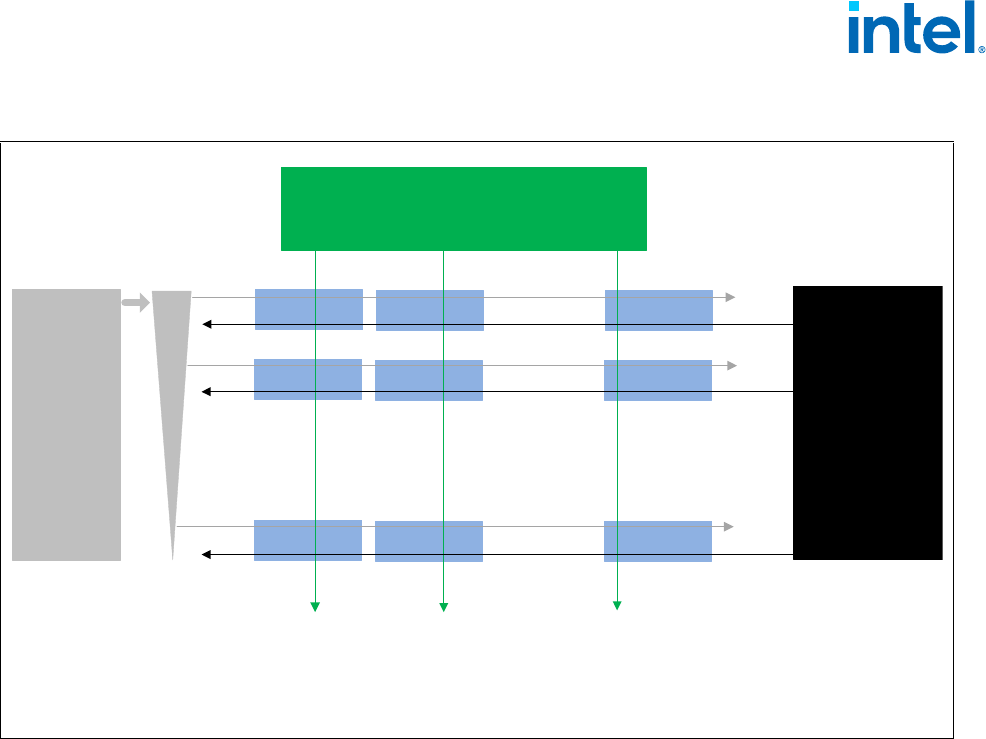
Document Number: 319433-052 3-3
INTEL® AMX INSTRUCTION SET REFERENCE, A-Z
The number of elements specified by colsb of the B matrix is also less than or equal to tmul_maxn. Any remaining
values beyond that specified by the metadata will be set to zero.
The XSAVE feature sets supports context management of the new state defined for Intel AMX. This support is
described in Section 3.2.
3.1.1 Tile Architecture Details
The supported parameters for the tile architecture are reported via CPUID; this includes information about how the
number of tile registers (max_names) can be configured (the palette). Configuring the tile architecture is intended
to be done once when entering a region of tile code using the LDTILECFG instruction specifying the selected palette
and describing in detail the configuration for each tile. Incorrect assignments will result in a General Protection fault
(#GP). Successful LDTILECFG initializes (zeroes) TILEDATA.
Exiting a tile region is done with the TILERELEASE instruction. It takes no parameters and invalidates all tiles (indi-
cating that the data no longer needs any saving or restoring). Essentially, it is an optimization of LDTILECFG with
an implicit palette of 0.
For applications that execute consecutive Intel AMX regions with differing configurations, TILERELEASE is not
required between them since the second LDTILECFG will clear all the data while loading the new configuration.
There is no instruction set support for automatic nesting of tile regions, though with sufficient effort software can
accomplish this by saving and restoring TILEDATA and TILECFG either through the XSAVE architecture or the Intel
AMX instructions.
The tile architecture boots in its INIT state, with TILECFG and TILEDATA set to zero. A successfully executing LDTI-
LECFG instruction to a non-zero palette sets the TILES_CONFIGURED=1, indicating the TILECFG is not in the INIT
state. The TILERELEASE instruction sets TILES_CONFIGURED = 0 and initializes (zeroes) TILEDATA.
Figure 3-2. The TMUL Unit
C[M][N]
B[K][N]
. . . .
FMA.0.N-1
. . . .
FMA.1.N-1
FMA.K-1.N-1
A[M][K]
FMA.0.0
. . . .
FMA.1.0
FMA.K-1.0
FMA.0.1
. . . .
FMA.1.1
FMA. K-1.1
A[m-1][1]
A[m][0]
. . . .
. . . .
A[m-K+1][K-1]
C[m][n-1]
C[m-K+1][n-1]
C[m][1]
C[m-K+1][1]
C[m][0]
C[m-K+1][0]
B[0][:N]
B[1][:N]
B[K-1][:N]
for m < M: // time steps
for k < K: // grid height
for n < N: // SIMD dimension
C[m][n] += VNNI_MUL(A[m][k], B[k][n])
Document Number: 319433-052 3-4
INTEL® AMX INSTRUCTION SET REFERENCE, A-Z
To facilitate handling of tile configuration data, there is a STTILECFG instruction. If the tile configuration is in the
INIT state (TILES_CONFIGURED == 0), then STTILECFG will write 64 bytes of zeros. Otherwise STTILECFG will
store the TILECFG to memory in the format used by LDTILECFG.
3.1.2 TMUL Architecture Details
The supported parameters for the TMUL architecture are reported via CPUID; see “CPUID—CPU Identification” in
Chapter 1, page 1-26, for details. These parameters include a maximum height (tmul_maxk) and a maximum
SIMD dimension (tmul_maxn). The metadata that accompanies the srcdest, src1 and src2 tiles to the TMUL unit
will be dynamically checked to see that they match the TMUL unit support for the data type and match the require-
ments of a meaningful matrix multiplication.
Figure 3-3 shows an example of the inner loop of an algorithm of using the TMUL architecture to compute a matrix
multiplication. In this example, we use two result tiles, tmm0 and tmm1, from matrix C to accumulate the interme-
diate results. One tile from the A matrix (tmm2) is re-used twice as we multiply it by two tiles from the B matrix.
The algorithm then advances pointers to load a new A tile and two new B tiles from the directions indicated by the
arrows. An outer loop, not shown, adjusts the pointers for the C tiles.
Figure 3-3. Matrix Multiply C+= A*B
LDTILECFG [rax]
// assume some outer loops driving the cache tiling (not shown)
{
TILELOADD tmm0, [rsi+rdi] // srcdst, RSI points to C, RDI is strided value
TILELOADD tmm1, [rsi+rdi+N] // second tile of C, unrolling in SIMD dimension N
MOV r14, 0
LOOP:
TILELOADD tmm2, [r8+r9] // src2 is strided load of A, reused for 2 TMUL instr.
TILELOADD tmm3, [r10+r11] // src1 is strided load of B
TDPBUSD tmm0, tmm2, tmm3 // update left tile of C
TILELOADD tmm3, [r10+r11+N] // src1 loaded with B from next rightmost tile
TDPBUSD tmm1, tmm2, tmm3 // update right tile of C
ADD r8, K // update pointers by constants known outside of loop
ADD r10, K*r11
ADD r14, K
CMP r14, LIMIT
JNE LOOP
TILESTORED [rsi+rdi], tmm0 // update the C matrix in memory
TILESTORED [rsi+rdi+M], tmm1
} // end of outer loop
TILERELEASE // return tiles to INIT state
C B
A

Document Number: 319433-052 3-5
INTEL® AMX INSTRUCTION SET REFERENCE, A-Z
3.1.3 Handling of Tile Row and Column Limits
Intel AMX operations will zero any rows and any columns beyond the dimensions specified by TILECFG. Tile opera-
tions will zero the data beyond the configured number of column bytes as each row is written. For example, with
64-byte rows and a tile configured with 10 rows and 48 columns, an operation writing dword elements would write
each of the first 10 rows with 48 bytes of output/result data and zero the remaining 16 bytes in each row. Tile oper-
ations also fully zero any rows after the first 10 configured rows. When using a 1 KByte tile with 64-byte rows,
there would be 16 rows, so in this example, the last 6 rows would also be zeroed.
Intel AMX instructions will always obey the metadata on reads and the zeroing rules on writes, and so a subsequent
XSAVE would see zeros in the appropriate locations. Tiles that are not written by Intel AMX instructions between
XRSTOR and XSAVE will write back with the same image they were loaded with regardless of the value of TILECFG.
3.1.4 Exceptions and Interrupts
Tile instructions are restartable so that operations that access strided memory can restart after page faults. To
support restarting instructions after these events, the instructions store information in the TILECFG.start_row
register. TILECFG.start_row indicates the row that should be used for restart; i.e., it indicates next row after the
rows that have already been successfully loaded (on a TILELOAD) or written to memory (on a TILESTORE) and
prevents repeating work that was successfully done.
The TMUL instruction set is not sensitive to the TILECFG.start_row value; this is due to there not being TMUL
instructions with memory operands or any restartable faults.
3.2 OPERAND RESTRICTIONS
Floating-point exceptions, denormal handling, and floating-point rounding: some of the Intel AMX instructions
operate on floating-point values. These instructions all function as if floating-point exceptions are masked, and use
the round-to-nearest-even (RNE) rounding mode. They also do not set any of the floating-point exception flags in
MXCSR. Table 3-1 describes the treatment of denormal inputs and outputs for Intel AMX operations.
3.3 IMPLEMENTATION PARAMETERS
The parameters are reported via CPUID leaf 1DH. Index 0 reports all zeros for all fields.
Table 3-1. Intel® AMX Treatment of Denormal Inputs and Outputs
Data Type Denormal Input Denormal Output
FP16 Allowed N/A
FP32 Treated as zero Flushed to zero
BF16 Treated as zero N/A
define palette_table[id]:
uint16_t total_tile_bytes
uint16_t bytes_per_tile
uint16_t bytes_per_row
uint16_t max_names
uint16_t max_rows

Document Number: 319433-052 3-6
INTEL® AMX INSTRUCTION SET REFERENCE, A-Z
The tile parameters are set by LDTILECFG or XRSTOR* of TILECFG:
3.4 HELPER FUNCTIONS
The helper functions used in Intel AMX instructions are defined below.
define tile[tid]:
byte rows
word colsb // bytes_per_row
bool valid
define write_row_and_zero(treg, r, data, nbytes):
for j in 0 ... nbytes-1:
treg.row[r].byte[j] := data.byte[j]
// zero the rest of the row
for j in nbytes ... palette_table[tilecfg.palette_id].bytes_per_row-1:
treg.row[r].byte[j] := 0
define zero_upper_rows(treg, r):
for i in r ... palette_table[tilecfg.palette_id].max_rows-1:
for j in 0 ... palette_table[tilecfg.palette_id].bytes_per_row-1:
treg.row[i].byte[j] := 0
define zero_tilecfg_start():
tilecfg.start_row := 0
define zero_all_tile_data():
if XCR0[TILEDATA]:
b := CPUID(0xD,TILEDATA).EAX // size of feature
for j in 0 ... b:
TILEDATA.byte[j] := 0

Document Number: 319433-052 3-7
INTEL® AMX INSTRUCTION SET REFERENCE, A-Z
3.5 NOTATION
Instructions described in this chapter follow the general documentation convention established in Intel
®
64 and IA-
32 Architectures Software Developer’s Manual Volume 2A. Additionally, Intel
®
Advanced Matrix Extensions use
notation conventions as described below.
In the instruction encoding boxes, sibmem is used to denote an encoding where a MODRM byte and SIB byte are
used to indicate a memory operation where the base and displacement are used to point to memory, and the index
register (if present) is used to denote a stride between memory rows. The index register is scaled by the sib.scale
field as usual. The base register is added to the displacement, if present.
In the instruction encoding, the MODRM byte is represented several ways depending on the role it plays. The
MODRM byte has 3 fields: 2-bit MODRM.MOD field, a 3-bit MODRM.REG field and a 3-bit MODRM.RM field. When all
bits of the MODRM byte have fixed values for an instruction, the 2-hex nibble value of that byte is presented after
the opcode in the encoding boxes on the instruction description pages. When only some fields of the MODRM byte
must contain fixed values, those values are specified as follows:
• If only the MODRM.MOD must be 0b11, and MODRM.REG and MODRM.RM fields are unrestricted, this is
denoted as 11:rrr:bbb. The rrr correspond to the 3-bits of the MODRM.REG field and the bbb correspond to
the 3-bits of the MODMR.RM field.
• If the MODRM.MOD field is constrained to be a value other than 0b11, i.e., it must be one of 0b00, 0b01, or
0b10, then we use the notation !(11).
• If the MODRM.REG field had a specific required value, e.g., 0b101, that would be denoted as mm:101:bbb.
NOTE
Historically the Intel
®
64 and IA-32 Architectures Software Developer’s Manual only specified the
MODRM.REG field restrictions with the notation /0 ... /7 and did not specify restrictions on the
MODRM.MOD and MODRM.RM fields in the encoding boxes.
3.6 EXCEPTION CLASSES
Alignment exceptions: The Intel AMX instructions that access memory will never generate #AC exceptions.
define xcr0_supports_palette(palette_id):
if palette_id == 0:
return 1
elif palette_id == 1:
if XCR0[TILECFG] and XCR0[TILEDATA]:
return 1
return 0

Document Number: 319433-052 3-8
INTEL® AMX INSTRUCTION SET REFERENCE, A-Z
Table 3-2. Intel® AMX Exception Classes
Class Description
AMX-E1
• #UD if preceded by LOCK, 66H, F2H, F3H or REX prefixes.
• #UD if CR4.OSXSAVE ≠ 1.
• #UD if XCR0[18:17]
≠ 0b11.
• #UD if IA32_EFER.LMA ≠ 1 OR CS.L ≠ 1.
• #UD if VVVV ≠ 0b1111.
• #GP based on palette and configuration checks (see pseudocode).
• #GP if the memory address is in a non-canonical form.
• #SS(0) if the memory address referencing the SS segment is in a non-canonical form.
• #PF if a page fault occurs.
AMX-E2
• #UD if preceded by LOCK, 66H, F2H, F3H or REX prefixes.
• #UD if CR4.OSXSAVE
≠ 1.
• #UD if XCR0[18:17] ≠ 0b11.
• #UD if IA32_EFER.LMA
≠ 1 OR CS.L ≠ 1.
• #UD if VVVV ≠ 0b1111.
• #GP if the memory address is in a non-canonical form.
• #SS(0) if the memory address referencing the SS segment is in a non-canonical form.
• #PF if a page fault occurs.
AMX-E3
• #UD if preceded by LOCK, 66H, F2H, F3H or REX prefixes.
• #UD if CR4.OSXSAVE
≠ 1.
• #UD if XCR0[18:17] ≠ 0b11.
• #UD if IA32_EFER.LMA
≠ 1 OR CS.L ≠ 1.
• #UD if VVVV ≠ 0b1111.
• #UD if not using SIB addressing.
• #UD if TILES_CONFIGURED == 0.
• #UD if tsrc or tdest are not valid tiles.
• #UD if tsrc/tdest are
≥ palette_table[tilecfg.palette_id].max_names.
• #UD if tsrc.colbytes mod 4
≠ 0 OR tdest.colbytes mod 4 ≠ 0.
• #UD if tilecfg.start_row ≥ tsrc.rows OR tilecfg.start_row ≥ tdest.rows.
• #GP if the memory address is in a non-canonical form.
• #SS(0) if the memory address referencing the SS segment is in a non-canonical form.
• #PF if any memory operand causes a page fault.
• #NM if XFD[18] == 1.

Document Number: 319433-052 3-9
INTEL® AMX INSTRUCTION SET REFERENCE, A-Z
3.7 INSTRUCTION SET REFERENCE
AMX-E4
• #UD if preceded by LOCK, 66H, F2H, F3H or REX prefixes.
• #UD if CR4.OSXSAVE ≠ 1.
• #UD if XCR0[18:17]
≠ 0b11.
• #UD if IA32_EFER.LMA ≠ 1 OR CS.L ≠ 1.
• #UD if srcdest == src1 OR src1 == src2 OR srcdest == src2.
• #UD if TILES_CONFIGURED == 0.
• #UD if srcdest.colbytes mod 4
≠ 0.
• #UD if src1.colbytes mod 4 ≠ 0.
• #UD if src2.colbytes mod 4
≠ 0.
• #UD if srcdest/src1/src2 are not valid tiles.
• #UD if srcdest/src1/src2 are ≥ palette_table[tilecfg.palette_id].max_names.
• #UD if srcdest.colbytes
≠ src2.colbytes.
• #UD if srcdest.rows ≠ src1.rows.
• #UD if src1.colbytes / 4 ≠ src2.rows.
• #UD if srcdest.colbytes > tmul_maxn.
• #UD if src2.colbytes > tmul_maxn.
• #UD if src1.colbytes/4 > tmul_maxk.
• #UD if src2.rows > tmul_maxk.
• #NM if XFD[18] == 1.
AMX-E5
• #UD if preceded by LOCK, 66H, F2H, F3H or REX prefixes.
• #UD if CR4.OSXSAVE
≠ 1.
• #UD if XCR0[18:17] ≠ 0b11.
• #UD if IA32_EFER.LMA ≠ 1 OR CS.L ≠ 1.
• #UD if VVVV
≠ 0b1111.
• #UD if TILES_CONFIGURED == 0.
• #UD if tdest is not a valid tile.
• #UD if tdest is
≥ palette_table[tilecfg.palette_id].max_names.
• #NM if XFD[18] == 1.
AMX-E6
• #UD if preceded by LOCK, 66H, F2H, F3H or REX prefixes.
• #UD if CR4.OSXSAVE
≠ 1.
• #UD if XCR0[18:17]
≠ 0b11.
• #UD if IA32_EFER.LMA ≠ 1 OR CS.L ≠ 1.
• #UD if VVVV ≠ 0b1111.
Table 3-2. Intel® AMX Exception Classes (Continued)
Class Description

Document Number: 319433-052 3-10
INTEL® AMX INSTRUCTION SET REFERENCE, A-Z
TCMMIMFP16PS/TCMMRLFP16PS—Matrix Multiplication of Complex Tiles Accumulated into
Packed Single Precision Tile
Instruction Operand Encoding
Description
These instructions perform matrix multiplication of two tiles containing complex elements and accumulate the
results into a packed single precision tile. Each dword element in input tiles tmm2 and tmm3 is interpreted as a
complex number with FP16 real part and FP16 imaginary part.
TCMMRLFP16PS calculates the real part of the result. For each possible combination of (row of tmm2, column of
tmm3), the instruction performs a set of multiplication and accumulations on all corresponding complex numbers
(one from tmm2 and one from tmm3). The real part of the tmm2 element is multiplied with the real part of the
corresponding tmm3 element, and the negated imaginary part of the tmm2 element is multiplied with the imagi-
nary part of the corresponding tmm3 elements. The two accumulated results are added, and then accumulated
into the corresponding row and column of tmm1.
TCMMIMFP16PS calculates the imaginary part of the result. For each possible combination of (row of tmm2, column
of tmm3), the instruction performs a set of multiplication and accumulations on all corresponding complex
numbers (one from tmm2 and one from tmm3). The imaginary part of the tmm2 element is multiplied with the real
part of the corresponding tmm3 element, and the real part of the tmm2 element is multiplied with the imaginary
part of the corresponding tmm3 elements. The two accumulated results are added, and then accumulated into the
corresponding row and column of tmm1.
“Round to nearest even” rounding mode is used when doing each accumulation of the FMA. Output denormals are
always flushed to zero but FP16 input denormals are not treated as zero.
MXCSR is not consulted nor updated.
Any attempt to execute these instructions inside an Intel TSX transaction will result in a transaction abort.
Operation
TCMMIMFP16PS tsrcdest, tsrc1, tsrc2
// C = m x n (tsrcdest), A = m x k (tsrc1), B = k x n (tsrc2)
# src1 and src2 elements are pairs of fp16
elements_src1 := tsrc1.colsb / 4
elements_dest := tsrcdest.colsb / 4
elements_temp := tsrcdest.colsb / 2 // Count is in fp16 prior to horizontal
for m in 0 ... tsrcdest.rows-1:
temp1[ 0 ... elements_temp-1] := 0
for k in 0 ... elements_src1-1:
for n in 0 ... elements_dest-1:
Opcode/
Instruction
Op/
En
64/32
bit Mode
Support
CPUID Feature
Flag
Description
VEX.128.66.0F38.W0 6C 11:rrr:bbb
TCMMIMFP16PS tmm1, tmm2, tmm3
AV/N.E. AMX-COMPLEX Matrix multiply complex elements from tmm2 and
tmm3, and accumulate the imaginary part into
single precision elements in tmm1.
VEX.128.NP.0F38.W0 6C 11:rrr:bbb
TCMMRLFP16PS tmm1, tmm2,
tmm3
AV/N.E. AMX-COMPLEX Matrix multiply complex elements from tmm2 and
tmm3, and accumulate the real part into single
precision elements in tmm1.
Op/En Tuple Operand 1 Operand 2 Operand 3 Operand 4
A N/A ModRM:reg (r, w) ModRM:r/m (r) VEX.vvvv (r) N/A

Document Number: 319433-052 3-11
INTEL® AMX INSTRUCTION SET REFERENCE, A-Z
s1e = cvt_fp16_to_fp32(tsrc1.row[m].fp16[2*k+0]) // real
s2e = cvt_fp16_to_fp32(tsrc2.row[k].fp16[2*n+0]) // real
s1o = cvt_fp16_to_fp32(tsrc1.row[m].fp16[2*k+1]) // imaginary
s2o = cvt_fp16_to_fp32(tsrc2.row[k].fp16[2*n+1]) // imaginary
// FP32 FMA with DAZ=FTZ=1, RNE rounding.
// MXCSR is neither consulted nor updated.
// No exceptions raised or denoted.
temp1.fp32[2*n+0] = fma32(temp1.fp32[2*n+0], s1o, s2e, daz=1, ftz=1, sae=1, rc=RNE)
temp1.fp32[2*n+1] = fma32(temp1.fp32[2*n+1], s1e, s2o, daz=1, ftz=1, sae=1, rc=RNE)
for n in 0 ... elements_dest-1:
// DAZ=FTZ=1, RNE rounding.
// MXCSR is neither consulted nor updated.
// No exceptions raised or denoted.
tmpf32 := temp1.fp32[2*n] + temp1.fp32[2*n+1]
srcdest.row[m].fp32[n] := srcdest.row[m].fp32[n] + tmpf32
write_row_and_zero(tsrcdest, m, tmp, tsrcdest.colsb)
zero_upper_rows(tsrcdest, tsrcdest.rows)
zero_tileconfig_start()
TCMMRLFP16PS tsrcdest, tsrc1, tsrc2
// C = m x n (tsrcdest), A = m x k (tsrc1), B = k x n (tsrc2)
# src1 and src2 elements are pairs of fp16
elements_src1 := tsrc1.colsb / 4
elements_dest := tsrcdest.colsb / 4
elements_temp := tsrcdest.colsb / 2 // Count is in fp16 prior to horizontal
for m in 0 ... tsrcdest.rows-1:
temp1[ 0 ... elements_temp-1 ] := 0
for k in 0 ... elements_src1-1:
for n in 0 ... elements_dest-1:
s1e = cvt_fp16_to_fp32(tsrc1.row[m].fp16[2*k+0]) // real
s2e = cvt_fp16_to_fp32(tsrc2.row[k].fp16[2*n+0]) // real
s1o = cvt_fp16_to_fp32(-tsrc1.row[m].fp16[2*k+1]) // imaginary: “-” is for imaginary*imaginary
s2o = cvt_fp16_to_fp32(tsrc2.row[k].fp16[2*n+1]) // imaginary
// FP32 FMA with DAZ=FTZ=1, RNE rounding.
// MXCSR is neither consulted nor updated.
// No exceptions raised or denoted.
temp1.fp32[2*n+0] = fma32(temp1.fp32[2*n+0], s1e, s2e, daz=1, ftz=1, sae=1, rc=RNE) // real
temp1.fp32[2*n+1] = fma32(temp1.fp32[2*n+1], s1o, s2o, daz=1, ftz=1, sae=1, rc=RNE) // imaginary
for n in 0 ... elements_dest-1:
// DAZ=FTZ=1, RNE rounding.
// MXCSR is neither consulted nor updated.
// No exceptions raised or denoted.
tmpf32 := temp1.fp32[2*n] + temp1.fp32[2*n+1]

Document Number: 319433-052 3-12
INTEL® AMX INSTRUCTION SET REFERENCE, A-Z
srcdest.row[m].fp32[n] := srcdest.row[m].fp32[n] + tmpf32
write_row_and_zero(tsrcdest, m, tmp, tsrcdest.colsb)
zero_upper_rows(tsrcdest, tsrcdest.rows)
zero_tileconfig_start()
Flags Affected
None.
Exceptions
AMX-E4; see Section 3.6, “Exception Classes” for details.

Document Number: 319433-052 3-13
INTEL® AMX INSTRUCTION SET REFERENCE, A-Z
TDPFP16PS—Dot Product of FP16 Tiles Accumulated into Packed Single Precision Tile
Instruction Operand Encoding
Description
This instruction performs a set of SIMD dot-products of two FP16 elements and accumulates the results into a
packed single precision tile. Each dword element in input tiles tmm2 and tmm3 is interpreted as a FP16 pair. For
each possible combination of (row of tmm2, column of tmm3), the instruction performs a set of SIMD dot-products
on all corresponding FP16 pairs (one pair from tmm2 and one pair from tmm3), adds the results of those dot-prod-
ucts, and then accumulates the result into the corresponding row and column of tmm1.
“Round to nearest even” rounding mode is used when doing each accumulation of the Fused Multiply-Add (FMA).
Output FP32 denormals are always flushed to zero. Input FP16 denormals are always handled and not treated as
zero.
MXCSR is not consulted nor updated.
Any attempt to execute the TDPFP16PS instruction inside an Intel TSX transaction will result in a transaction abort.
Operation
TDPFP16PS tsrcdest, tsrc1, tsrc2
// C = m x n (tsrcdest), A = m x k (tsrc1), B = k x n (tsrc2)
# src1 and src2 elements are pairs of fp16
elements_src1 := tsrc1.colsb / 4
elements_src2 := tsrc2.colsb / 4
elements_dest := tsrcdest.colsb / 4
elements_temp := tsrcdest.colsb / 2 // Count is in fp16 prior to horizontal
for m in 0 ... tsrcdest.rows-1:
temp1[ 0 ... elements_temp-1 ] := 0
for k in 0 ... elements_src1-1:
for n in 0 ... elements_dest-1:
// For this operation:
// Handle FP16 denorms. Not forcing input FP16 denorms to 0.
// FP32 FMA with DAZ=FTZ=1, RNE rounding.
// MXCSR is neither consulted nor updated.
// No exceptions raised or denoted.
temp1.fp32[2*n+0] += cvt_fp16_to_fp32(tsrc1.row[m].fp16[2*k+0]) *cvt_fp16_to_fp32(tsrc2.row[k].fp16[2*n+0])
temp1.fp32[2*n+1] += cvt_fp16_to_fp32(tsrc1.row[m].fp16[2*k+1]) *cvt_fp16_to_fp32(tsrc2.row[k].fp16[2*n+1])
for n in 0 ... elements_dest-1:
// DAZ=FTZ=1, RNE rounding.
// MXCSR is neither consulted nor updated.
Opcode/
Instruction
Op/
En
64/32
bit Mode
Support
CPUID Feature
Flag
Description
VEX.128.F2.0F38.W0 5C 11:rrr:bbb
TDPFP16PS tmm1, tmm2, tmm3
A V/N.E. AMX-FP16 Matrix multiply FP16 elements from tmm2 and
tmm3, and accumulate the packed single precision
elements in tmm1.
Op/En Tuple Operand 1 Operand 2 Operand 3 Operand 4
A N/A ModRM:reg (r, w) ModRM:r/m (r) VEX.vvvv (r) N/A

Document Number: 319433-052 3-14
INTEL® AMX INSTRUCTION SET REFERENCE, A-Z
// No exceptions raised or denoted.
tmpf32 := temp1.fp32[2*n] + temp1.fp32[2*n+1]
srcdest.row[m].fp32[n] := srcdest.row[m].fp32[n] + tmpf32
write_row_and_zero(tsrcdest, m, tmp, tsrcdest.colsb)
zero_upper_rows(tsrcdest, tsrcdest.rows)
zero_tileconfig_start()
Flags Affected
None.
Exceptions
AMX-E4; see Section 3.6, “Exception Classes” for details.

Document Number: 319433-052 4-1
UC-LOCK DISABLE
CHAPTER 4
UC-LOCK DISABLE
4.1 FEATURES TO DISABLE BUS LOCKS
Processors will assert a bus lock for a locked access in either of the following situations: (1) the access is to
multiple cache lines (a split lock); or (2) the access with a me mory type other than WB (a UC lock)
1
. Because bus
locks may adversely affect performance in certain situations, processors may support two features that system
software can use to disable bus locking. These are called split-lock disable and UC-lock disable.
A processor enumerates support for split-lock disable by setting bit 5 of the IA32_CORE_CAPABILITIES MSR (MSR
index CFH). If this bit is read as 1, software can enable split-lock disable by setting bit 29 of the MSR_MEMO-
RY_CTRL MSR (MSR index 33H). When this bit is set, a locked access to multiple cache lines causes an alignment-
check exception (#AC) with a zero error code.
2
The locked access does not occur.
While MSR_MEMORY_CTRL is not an architectural MSR, the behavior split-lock disable is consistent across
processor models that enumerate support for it in the IA32_CORE_CAPABILITIES MSR.
Support for UC-lock disable is detailed in Section 4.2.
4.2 UC-LOCK DISABLE
A processor enumerates support for UC-lock disable either by setting IA32_CORE_CAPABILITIES[4] or by enumer-
ating CPUID.(EAX=07H, ECX=2):EDX[bit 6] as 1. The latter form of enumeration (CPUID) is used beginning with
processors based on Sierra Forest microarchitecture or Grand Ridge microarchitecture; earlier processors may use
the former form (IA32_CORE_CAPABILITIES).
NOTE
No processor will both set IA32_CORE_CAPABILITIES[4] and enumerate
CPUID.(EAX=07H, ECX=2):EDX[bit 6] as 1.
If a processor enumerates support for UC-lock disable (in either way), software can enable UC-lock disable by
setting MSR_MEMORY_CTRL[28]. When this bit is set, a locked access using a memory type other than WB causes
a fault. The locked access does not occur. The specific fault that occurs depends on how UC-lock disable is enumer-
ated:
• If IA32_CORE_CAPABILITIES[4] is read as 1, the UC lock results in a general-protection exception (#GP) with
a zero error code.
• If CPUID.(EAX=07H, ECX=2):EDX[bit 6] is enumerated as 1, the UC lock results in an #AC with an error code
with value 4.
1. The term “UC lock” is used because the most common situation regards accesses to UC memory. Despite the name, locked accesses
to WC, WP, and WT memory also cause bus locks.
2. Other alignment-check exceptions occur only if CR0.AM = 1, EFLAGS.AC = 1, and CPL = 3. The alignment-check exceptions resulting
from split-lock disable may occur even if CR0.AM = 0, EFLAGS.AC = 0, or CPL < 3.

Document Number: 319433-052 4-2
UC-LOCK DISABLE
Table 4-1. MEMORY_CTRL MSR
Register Address
Architectural MSR Name / Bit Fields Description
Hex Decimal
33H 51 MSR_MEMORY_CTRL Memory Control Register
27:0 Reserved
28 UC_LOCK_DISABLE
If set to 1 and CPUID.(EAX=07H, ECX=2):EDX[6] = 0, a UC lock
will cause a #GP(0) exception.
If set to 1 and CPUID.(EAX=07H, ECX=2):EDX[6] = 1, a UC lock
will cause an #AC(4) exception.
29 SPLIT_LOCK_DISABLE
If set to 1, a split lock will cause an #AC(0) exception.
31:30 Reserved

Document Number: 319433-052 5-1
INTEL® RESOURCE DIRECTOR TECHNOLOGY FEATURE UPDATES
CHAPTER 5
INTEL® RESOURCE DIRECTOR TECHNOLOGY FEATURE UPDATES
Intel
®
Resource Director Technology (Intel
®
RDT) provides several monitoring and control capabilities for shared
resources in multiprocessor systems. This chapter covers updates to the Cache Bandwidth Allocation feature of
Intel RDT.
Previous versions of this document contained additional information on Intel RDT. This information can now be
found in the Intel® 64 and IA-32 Architectures Software Developer’s Manual, Volume 3B, as well as in a new docu-
ment titled “Intel® Resource Director Technology Architecture Specification,” available here:
https://cdrdv2.intel.com/v1/dl/getContent/789566
.
5.1 CACHE BANDWIDTH ALLOCATION (CBA)
5.1.1 Introduction to Cache Bandwidth Allocation
The Cache Bandwidth Allocation (CBA) feature provides control over bandwidth available between Level 1 (L1)
caches, Level 2 (L2) Caches, and Level 3 (L3) Caches (as applicable) for each of the logical processors. Since
reducing upstream bandwidth can also reduce bandwidth to external memory, this also provides an indirect control
of memory bandwidth. The CBA feature, along with the MBA, provides a mechanism to control the bandwidth of
different applications.
A given CLOS used for L3 CAT, for instance, means the same thing as a CLOS used for CBA. Infrastructure such as
the MSR used to associate a logical processor with a CLOS (the IA32_PQR_ASSOC_MSR) and some elements of the
CPUID enumeration (such as CPUID leaf 10H (Cache Allocation Technology Enumeration Leaf)) are shared. For
more information, refer to the “Intel® Resource Director Technology Architecture Specification.”
The following sections describe the CPUID enumeration and configuration interfaces (Model-Specific Registers)
applicable to the Cache Bandwidth Allocation feature.
5.1.2 Cache Bandwidth Allocation Enumeration
As with certain other Intel RDT features, enumeration of the presence and details of the CBA feature is provided via
a sub-leaf of the CPUID instruction.
Key components of the enumeration include support for the CBA feature on the processor, and if CBA is supported,
the following details:
• Number of supported Classes of Service for the processor.
• Scope of the CBA feature MSRs.
• The maximum CBA throttle Level supported.
• An indication of whether the throttle values that can be programmed are linearly spaced or not.
The presence of any of the Intel RDT features that enable control over shared platform resources is enumerated by
executing CPUID instruction with EAX = 07H and ECX = 0H as input. If CPUID.(EAX=07H, ECX=0H):EBX.PQE[bit
15] reports 1, the processor supports software control over shared processor resources. Software may then use
CPUID leaf 10H to enumerate additional details on the specific controls provided.
Using CPUID leaf 10H, software may determine whether CBA is supported on the platform. Specifically, as shown
in Figure 17-31, bit 5 of the EBX register indicates whether CBA is supported on the processor, and the bit position
(5) constitutes a Resource ID (ResID), which allows the enumeration of CBA details. For instance, if bit 5 is
supported, this implies the presence of CPUID.10H.[ResID=5] as shown in CPUID.(EAX=10H, ECX=5H), CBA
Feature Details Identification, which provides the following details (this information can also be found in Table 1-3,
“Information Returned by CPUID Instruction”):

Document Number: 319433-052 5-2
INTEL® RESOURCE DIRECTOR TECHNOLOGY FEATURE UPDATES
• CPUID.(EAX=10H, ECX=ResID=5):EAX
— EAX[7:0] reports the maximum CBA throttling value supported.
— EAX[11:8] reports the scope of CBA IA32_QoS_Core_BW_Thrtl_n MSRs. If EAX[11:8]=1, this indicates the
logical processor scope of the MSRs.
— EAX[31:12] is reserved.
• CPUID.(EAX=10H, ECX=ResID=5):EBX
— EBX[31:0] is reserved.
• CPUID.(EAX=10H, ECX=ResID=5):ECX
— ECX[3] reports whether the response of the bandwidth control is approximately linear. If ECX[3] is 1, the
response of the bandwidth control is approximately linear. If ECX[3] is 0, the response of the bandwidth
control is non-linear.
— ECX[2:0] and ECX[31:4] are reserved.
• CPUID.(EAX=10H, ECX=ResID=5):EDX
— EDX[15:0] reports the number of Classes of Service supported for the feature. Add one to the return value
to get the result. For instance, a reported value of 15 implies a maximum of 16 supported CBA CLOS.
— EDX[31:16] is reserved.
Figure 5-1. CPUID.(EAS=10H, ECX=5H), CBA Feature Details Identification
0
31
Reserved
0
31
3
2
31 12 11 8 7 0
Reserved
ECX
EBX
EAX
CBA_MAX_Throttle_Level
31 16 15 0
Reserved
CLOS_MAX
EDX
CPUID.(EAX = 10H, ECX = ResID = 5) Output:
Reserved
CBA_Lin_Rsp
Scope of
CBA MSRs

Document Number: 319433-052 5-3
INTEL® RESOURCE DIRECTOR TECHNOLOGY FEATURE UPDATES
5.1.3 Cache Bandwidth Allocation Configuration
The configuration of CBA consists of two processes once enumeration is complete:
• The association of logical processors to Classes of Service (CLOS) is accomplished commonly across Intel RDT
features through the IA32_PQR_ASSOC MSR. Software may update the CLOS field of the PQR MSR dynami-
cally, including at context swap time, to maintain the proper association of logical processors to Classes of
Service on the hardware.
• A new set of architectural MSRs is added to enable software to communicate the memory bandwidth QoS
requirements of the application running on the logical processor. The scope of these MSRs,
IA32_QoS_Core_BW_Thrtl_n, is per logical processor. Each MSR encodes packed 8-bit fields indexed by Class
of Service, which specify the Throttle Level for each CLOS.
The CLOS field value of the IA32_PQR_ASSOC MSR is used to index into the MSRs and select the software-specified
Throttle Level. Each logical processor uses this level to control the bandwidth across the cache hierarchy. The hard-
ware ensures coordination with the MBA feature (where present). The reset value of the CLOS[i].Level=0 indicates
unthrottled bandwidth. This field may be programmed from 0 to CBA_MAX_Throttle_Level (see Figure 5-1). Any
values outside this range will generate a #GP(0). A higher value of CLOS[i].Level implies a higher level of band-
width throttling, and a lower number indicates lesser throttling. The number of supported CLOS for a given logical
processor is enumerated in CPUID.(EAX=10H, ECX=5H):EDX. In an example where a logical processor supports 16
CLOS, two 64-bit MSRs with packed Throttling Levels (TLs) are defined, IA32_QoS_Core_BW_Thrtl_0 (defining
packed TLs for CLOS[7:0]) and IA32_QoS_Core_BW_Thrtl_1 (defining TLs for CLOS[15:8]). For example, within
the MSR IA32_QoS_Core_BW_Thrtl_0, bits [7:0] define the TL field for CLOS 0 (see Figure 5-2).
Advanced versions of the MBA feature may manage the external memory bandwidth associated with the CLOS by
dynamically increasing or decreasing the bandwidth, under software guidance, to maintain throttling priorities
while maximizing system performance as described in the Intel Software Developer's Manual and the Intel RDT
Architecture Specification. The CBA feature, along with the MBA, provides a mechanism to control the bandwidth
of different applications. Software should understand that the effective throttling of an application may be which-
ever of the CBA or MBA specifies more throttling. Software may use CBA, MBA, or a combination to achieve band-
width and performance management goals if supported on a processor.
Table 5-1. Cache Bandwidth Allocation (CBA) MSRs
Delay Value MSR Address
IA32_QoS_Core_BW_Thrtl_0 E00H
IA32_QoS_Core_BW_Thrtl_1 E01H
IA32_QoS_Core_BW_Thrtl_2 E02H
... ...
IA32_QoS_Core_BW_Thrtl _'(((COS_MAX+1)/8) - 1)' E00H + ((COS_MAX from CPUID.10H.5 + 1)/8 - 1)

Document Number: 319433-052 5-4
INTEL® RESOURCE DIRECTOR TECHNOLOGY FEATURE UPDATES
Note that the throttling values provided to the software are calibrated through specific traffic patterns; however, as
workload characteristics may vary, the response precision and linearity of the bandwidth threshold values will vary
across products and should be treated as approximate values only.
5.1.4 Cache Bandwidth Allocation Usage Considerations
Cache Bandwidth Allocation has various software usage considerations and improves efficiency over product
generations. See the “Intel® Resource Director Technology Architecture Specification” for additional details.
Figure 5-2. IA32_QoS_Core_BW_Thrtl_n MSR Definition
0
63
IA32_QoS_Core_BW_Thrtl_0 MSR
[63:56] [55:48]
[47:40]
[39:32] [31:24]
[23:16]
[15:8]
[7:0]
CLOS[7].Level
CLOS[6].Level
CLOS[5].Level
CLOS[4].Level
CLOS[3].Level
CLOS[2].Level
CLOS[1].Level
CLOS[0].Level
Base MSR Address = E00H
0
63
IA32_QoS_Core_BW_Thrtl_1 MSR
[63:56] [55:48]
[47:40]
[39:32] [31:24]
[23:16]
[15:8]
[7:0]
CLOS[15].Level
CLOS[14].Level
CLOS[13].Level
CLOS[12].Level
CLOS[11].Level
CLOS[10].Level
CLOS[9].Level
CLOS[8].Level
Base MSR Address = E01H

Document Number: 319433-052 6-1
LINEAR ADDRESS MASKING (LAM)
CHAPTER 6
LINEAR ADDRESS MASKING (LAM)
This chapter describes a new feature called linear-address masking (LAM). LAM modifies the checking that is
applied to 64-bit linear addresses, allowing software to use of the untranslated address bits for metadata.
In 64-bit mode, linear address have 64 bits and are translated either with 4-level paging, which translates the low
48 bits of each linear address, or with 5-level paging, which translates 57 bits. The upper linear-address bits are
reserved through the concept of canonicality. A linear address is 48-bit canonical if bits 63:47 of the address are
identical; it is 57-bit canonical if bits 63:56 are identical. (Clearly, any linear address that is 48-bit canonical is also
57-bit canonical.) When 4-level paging is active, the processor requires all linear addresses used to access memory
to be 48-bit canonical; similarly, 5-level paging ensures that all linear addresses are 57-bit canonical.
Software usages that associate metadata with a pointer might benefit from being able to place metadata in the
upper (untranslated) bits of the pointer itself. However, the canonicality enforcement mentioned earlier implies
that software would have to mask the metadata bits in a pointer (making it canonical) before using it as a linear
address to access memory. LAM allows software to use pointers with metadata without having to mask the meta-
data bits. With LAM enabled, the processor masks the metadata bits in a pointer before using it as a linear address
to access memory.
LAM is supported only in 64-bit mode and applies only addresses used for data accesses. LAM does not apply to
addresses used for instruction fetches or to those being loaded into the RIP register (e.g., as targets of jump and
call instructions).
6.1 ENUMERATION, ENABLING, AND CONFIGURATION
LAM support by the processor is enumerated by the CPUID feature flag CPUID.(EAX=07H, ECX=01H):EAX.LAM[bit
26]. Enabling and configuration of LAM is controlled by the following new bits in control registers: CR3[62]
(LAM_U48), CR3[61] (LAM_U57), and CR4[28] (LAM_SUP). The use of these control bit is explained below.
LAM supports configurations that differ regarding which pointer bits are masked and can be used for metadata.
With LAM48, pointer bits in positions 62:48 are masked (resulting in a LAM width of 15); with LAM57, pointer
bits in positions 62:57 are masked (a LAM width of 6). The LAM width may be configured differently for user and
supervisor pointers. LAM identifies pointer as a user pointer if bit 63 of the pointer is 0 and as a supervisor pointer
if bit 63 of the pointer is 1.
CR3.LAM_U48 and CR3.LAM_U57 enable and configure LAM for user pointers:
• If CR3.LAM_U48 = CR3.LAM_U57 = 0, LAM is not enabled for user pointers.
• If CR3.LAM_U48 = 1 and CR3.LAM_U57 = 0, LAM48 is enabled for user pointers (a LAM width of 15).
• If CR3.LAM_U57 = 1, LAM57 applies to user pointers (a LAM width of 6; CR3.LAM_U48 is ignored).
CR4.LAM_SUP enables and configures LAM for supervisor pointers:
• If CR4.LAM_SUP = 0, LAM is not enabled for supervisor pointers.
• If CR4.LAM_SUP = 1, LAM is enabled for supervisor pointers with a width determined by the paging mode:
— If 4-level paging is enabled, LAM48 is enabled for supervisor pointers (a LAM width of 15).
— If 5-level paging is enabled, LAM57 is enabled for supervisor pointers (a LAM width of 6).
Note that the LAM identification of a pointer as user or supervisor is based solely on the value of pointer bit 63 and
does not, for the purposes of LAM, depend on the CPL.
6.2 TREATMENT OF DATA ACCESSES WITH LAM ACTIVE FOR USER POINTERS
Recall that, without LAM, canonicality checks are defined so that 4-level paging requires bits 63:47 of each pointer
to be identical, while 5-level paging requires bits 63:56 to be identical. LAM allows some of these bits to be used as
metadata by modifying canonicality checking.

Document Number: 319433-052 6-2
LINEAR ADDRESS MASKING (LAM)
When LAM48 is enabled for user pointers (see Section 6.1), the processor allows bits 62:48 of a user pointer to be
used as metadata. Regardless of the paging mode, the processor performs a modified canonicality check that
enforces that bit 47 of the pointer matches bit 63. As illustrated in Figure 6-1, bits 62:48 are not checked and are
thus available for software metadata. After this modified canonicality check is performed, bits 62:48 are masked
by sign-extending the value of bit 47 (0), and the resulting (48-bit canonical) address is then passed on for trans-
lation by paging.
(Note also that, without LAM, canonicality checking with 5-level paging does not apply to bit 47 of a user pointer;
when LAM48 is enabled for user pointers, bit 47 of a user pointer must be 0. Note also that linear-address
bits 56:47 are translated by 5-level paging. When LAM48 is enabled for user pointers, these bits are always 0 in
any linear address derived from a user pointer: bits 56:48 of the pointer contained metadata, while bit 47 is
required to be 0.)
When LAM57 is enabled for user pointers, the processor allows bits 62:57 of a user pointer to be used as metadata.
With 5-level paging, the processor performs a modified canonicality check that enforces only that bit 56 of the
pointer matches bit 63. As illustrated in Figure 6-2, bits 62:57 are not checked and are thus available for software
metadata. After this modified canonicality check is performed, bits 62:57 are masked by sign-extending the value
of bit 56 (0), and the resulting (57-bit canonical) address is then passed on for translation by 5-level paging.
When LAM57 is enabled for user pointers with 4-level paging, the processor performs a modified canonicality check
that enforces only that bits 56:47 of a user pointer match bit 63. As illustrated in Figure 6-3, bits 62:57 are not
checked and are thus available for software metadata. After this modified canonicality check is performed, bits
62:57 are masked by sign-extending the value of bit 56 (0), and the resulting (48-bit canonical) address is then
passed on for translation by 4-level paging.
Figure 6-1. Canonicality Check When LAM48 is Enabled for User Pointers
Figure 6-2. Canonicality Check When LAM57 is Enabled for User Pointers with 5-Level Paging
063 62 48 47 46
SW Metadata
0 0
==
063 62 57 56 55
SW Metadata
0 0
==

Document Number: 319433-052 6-3
LINEAR ADDRESS MASKING (LAM)
6.3 TREATMENT OF DATA ACCESSES WITH LAM ACTIVE FOR SUPERVISOR
POINTERS
As with user pointers (Section 6.2), LAM can be configured to modify canonicality checking to allow use of meta-
data in supervisor pointers. For supervisor pointers, the number of metadata bits (the LAM width) available
depends on the paging mode active: with 5-level paging, enabling LAM for supervisor pointers results in LAM57;
with 4-level paging, it results in LAM48 (see Section 6.1).
When LAM57 is enabled for supervisor pointers (5-level paging), the processor performs a modified canonicality
check that enforces only that bit 56 of a supervisor pointer matches bit 63. As illustrated in Figure 6-4, bits 62:57
are not checked and are thus available for software metadata. After this modified canonicality check is performed,
bits 62:57 are masked by sign-extending the value of bit 56 (1), and the resulting (57-bit canonical) address is
then passed on for translation by 5-level paging.
When LAM48 is enabled for supervisor pointers (4-level paging), the processor performs a modified canonicality
check that enforces only that bit 47 of a supervisor pointer matches bit 63. As illustrated in Figure 6-5, bits 62:48
are not checked and are thus available for software metadata. After this modified canonicality check is performed,
bits 62:48 are masked by sign-extending the value of bit 47 (1), and the resulting (48-bit canonical) address is
then passed on for translation by 4-level paging.
Figure 6-3. Canonicality Check When LAM57 is Enabled for User Pointers with 4-Level Paging
Figure 6-4. Canonicality Check When LAM57 is Enabled for Supervisor Pointers with 5-Level Paging
063 62 57 56 47 46
SW Metadata
0 0
==
063 62 57 56 55
SW Metadata
1 1
==

Document Number: 319433-052 6-4
LINEAR ADDRESS MASKING (LAM)
6.4 CANONICALITY CHECKING FOR DATA ADDRESSES WRITTEN TO CONTROL
REGISTERS AND MSRS
Processors that support LAM continue to require the addresses written to control registers or MSRs to be 57-bit
canonical if the processor supports 5-level paging or 48-bit canonical if it supports only 4-level paging; LAM
masking is not performed on these writes. Similarly, LAM masking does not apply to loads of the SSP register, nor
does it apply to loads of GDTR, IDTR, LDTR, and TR by LGDT, LIDT, LLDT, and LTR. When the contents of such regis-
ters are used as pointers to access memory, the processor performs canonicality checking and masking based on
paging mode and LAM mode configuration active at the time of access.
6.5 PAGING INTERACTIONS
As explained in Section 6.2 and Section 6.3, LAM masks certain bits in a pointer by sign-extension, resulting in a
linear address to be translated by paging.
In most cases, the address bits in the masked positions are not used by address translation. However, if 5-level
paging is active and LAM48 is enabled for user pointers, bit 47 of a user pointer must be zero and is extended over
bits 62:48 to form a linear address — even though bits 56:48 are used by 5-level paging. This implies that, when
LAM48 is enabled for user pointers, bits 56:47 are 0 in any linear address translated for a user pointer.
Page faults report the faulting linear address in CR2. Because LAM masking (by sign-extension) applies before
paging, the faulting linear address recorded in CR2 does not contain the masked metadata.
The INVLPG instruction is used to invalidate any translation lookaside buffer (TLB) entries for a memory address
specified with the source operand. LAM does not apply to the specified memory address. Thus, in 64-bit mode, if
the memory address specified is in non-canonical form then the INVLPG is the same as a NOP.
The INVPCID instruction invalidates mappings in the TLB and paging structure caches based on the processor
context identifier (PCID). The INVPCID descriptor provides the memory address to invalidate when the descriptor
is of type 0 (individual-address invalidation). LAM does not apply to the specified memory address, and in 64-bit
mode if this memory address is in non-canonical form then the processor generates a #GP(0) exception.
6.6 VMX INTERACTIONS
6.6.1 Guest Linear Address
Certain VM exits save in a VMCS field the guest linear address pertaining to the VM exit. Because such a linear
address results from masking the original pointer, the processor does not report the masked metadata in the
VMCS. The guest linear address saved is always the result of the sign-extension described in Section 6.2 and
Section 6.3.
Figure 6-5. Canonicality Check When LAM48 is Enabled for Supervisor Pointers with 4-Level Paging
063 62 48 47 46
SW Metadata
1 1
==

Document Number: 319433-052 6-5
LINEAR ADDRESS MASKING (LAM)
6.6.2 VM-Entry Checking of Values of CR3 and CR4
VM entry checks the values of the CR3 and CR4 fields in the guest-area and host-state area of the VMCS. In partic-
ular, the bits in these fields that correspond to bits reserved in the corresponding register are checked and must be
0.
On processors that enumerate support for LAM (Section 6.1), VM entry allows bits 62:61 to be set in either CR3
field and allows bit 28 to be set in either CR4 field.
6.6.3 CR3-Target Values
If the “CR3-load exiting” VM-execution control is 1, execution of MOV to CR3 in VMX non-root operation causes a
VM exit unless the value of the instruction’s source operand is equal to one of the CR3-target values specified in the
VMCS.
Processor support for LAM does not change this behavior. The comparison of the instruction source operand to each
of the CR3-target values considers all 64 bits, including the two new bits that determine LAM enabling for user
pointers (see Section 6.1).
6.6.4 Hypervisor-Managed Linear Address Translation (HLAT)
Hypervisor-managed linear-address translation (HLAT) is enabled when the “enable HLAT” tertiary processor-
based VM-execution control is 1.
When HLAT is enabled for a guest, the processor translates a linear address using HLAT paging structures (instead
of guest paging structures) if the address matches the Protected Linear Range (PLR). When LAM is active, it is the
linear address (derived from a pointer by masking) that is checked for a PLR match.
The hierarchy of HLAT paging structures is located using a guest-physical address in the VMCS (instead of the
guest-physical address in CR3). Nevertheless, LAM enabling and configuration for user pointers is based on the
value of CR3[62:61] (see Section 6.1) even when the guest-physical address in CR3 is not used for translating the
linear addresses derived from user pointers.
6.7 DEBUG AND TRACING INTERACTIONS
6.7.1 Debug Registers
Debug registers DR0-DR3 can be programmed with linear addresses that are matched against memory accesses
for data breakpoints or instruction breakpoints. When LAM is active, it is the linear address (derived from a pointer
by masking) that is checked for matching the contents of the debug registers.
6.7.2 Intel® Processor Trace
Intel Processor Trace supports a CR3-filtering mechanism by which generation of packets containing architectural
states can be enabled or disabled based on the value of CR3 matching the contents of the IA32_RTIT_CR3_MATCH
MSR. On processors that support LAM, bits 62:61 of the CR3 (see Section 6.1) must also match bits 62:61 of this
MSR to enable tracing.
6.8 INTEL® SGX INTERACTIONS
Memory operands of ENCLS, ENCLU, and ENCLV that are data pointers follow the LAM architecture and mask suit-
ably. Code pointers continue to not mask metadata bits. ECREATE does not mask BASEADDR specified in SECS,
and the unmasked BASEADDR must be canonical.
Two new SECS attribute bits are defined for LAM support in enclave mode:

Document Number: 319433-052 6-6
LINEAR ADDRESS MASKING (LAM)
• ATTRIBUTES.LAM_U48 (bit 9) - Activate LAM for user data pointers and use of bits 62:48 as masked metadata
in enclave mode. This bit can be set if CPUID.(EAX=12H, ECX=01H):EAX[9] is 1.
• ATTRIBUTES.LAM_U57 (bit 8) - Activate LAM for user data pointers and use of bits 62:57 as masked metadata
in enclave mode. This bit can be set if CPUID.(EAX=12H, ECX=01H):EAX[8] is 1.
ECREATE causes #GP(0) if ATTRIBUTE.LAM_U48 bit is 1 and CPUID.(EAX=12H, ECX=01H):EAX[9] is 0, or if
ATTRIBUTE.LAM_U57 bit is 1 and CPUID.(EAX=12H, ECX=01H):EAX[8] is 0.
During enclave execution, accesses using linear addresses are treated as if CR3.LAM_U48 =
SECS.ATTRIBUTES.LAM_U48, CR3.LAM_U57 = SECS.ATTRIBUTES.LAM_U57, and CR4.LAM_SUP = 0. The actual
value of CR3 is not changed. This implies that, during enclave execution, if SECS.ATTRIBUTES.LAM_U57 = 1,
LAM57 is enabled for user pointers during enclave execution and, if SECS.ATTRIBUTES.LAM_U57 = 0 and
SECS.ATTRIBUTES. LAM_U48 = 1, then LAM48 is enabled for user pointers. If SECS.ATTRIBUTES.LAM_U57 =
SECS.ATTRIBUTES. LAM_U48 = 0, LAM is not enabled for user pointers.
When in enclave mode, supervisor data pointers are not subject to any masking.
The following ENCLU leaf functions check for linear addresses to be within the ELRANGE. When LAM is active, this
check is performed on the linear addresses that result from masking metadata bits in user pointers used by the leaf
functions.
• EACCEPT
• EACCEPTCOPY
• EGETKEY
• EMODPE
• EREPORT
The following linear address fields in the Intel SGX data structures hold linear addresses that are either loaded into
the EPCM or are written out from the EPCM and do not contain any metadata.
• SECS.BASEADDR
• PAGEINFO.LINADDR
6.9 SYSTEM MANAGEMENT MODE (SMM) INTERACTIONS
On processors that enumerate support for LAM (Section 6.1), RSM allows restoring CR3 with a value that sets
either or both bit 62 and bit 61 and restoring a value of CR4 with a value that sets bit 28.

Document Number: 319433-052 7-1
CODE PREFETCH INSTRUCTION UPDATES
CHAPTER 7
CODE PREFETCH INSTRUCTION UPDATES
All changes to existing operation are highlighted in violet.
PREFETCHh—Prefetch Data or Code Into Caches
Instruction Operand Encoding
Description
Fetches the line of data or code (instructions’ bytes) from memory that contains the byte specified with the source
operand to a location in the cache hierarchy specified by a locality hint:
• T0 (temporal data)—prefetch data into all levels of the cache hierarchy.
• T1 (temporal data with respect to first level cache misses)—prefetch data into level 2 cache and higher.
• T2 (temporal data with respect to second level cache misses)—prefetch data into level 3 cache and higher, or
an implementation-specific choice.
• NTA (non-temporal data with respect to all cache levels)—prefetch data into non-temporal cache structure and
into a location close to the processor, minimizing cache pollution.
• IT0 (temporal code)—prefetch code into all levels of the cache hierarchy.
• IT1 (temporal code with respect to first level cache misses)—prefetch code into all but the first-level of the
cache hierarchy.
The source operand is a byte memory location. (The locality hints are encoded into the machine level instruction
using bits 3 through 5 of the ModR/M byte.) Some locality hints may prefetch only for RIP-relative memory
addresses; see additional details below. The address to prefetch is NextRIP + 32-bit displacement, where NextRIP
is the first byte of the instruction that follows the prefetch instruction itself.
If the line selected is already present in the cache hierarchy at a level closer to the processor, no data movement
occurs. Prefetches from uncacheable or WC memory are ignored.
Opcode/
Instruction
Op/
En
64/32 Bit
Mode
Support
Description
0F 18 /1
PREFETCHT0 m8
MV/V Move data from m8 closer to the processor using T0 hint.
0F 18 /2
PREFETCHT1 m8
MV/V Move data from m8 closer to the processor using T1 hint.
0F 18 /3
PREFETCHT2 m8
MV/V Move data from m8 closer to the processor using T2 hint.
0F 18 /0
PREFETCHNTA m8
MV/V Move data from m8 closer to the processor using NTA hint.
0F 18 /7
PREFETCHIT0 m8
M V/I Move code from relative address closer to the processor using IT0 hint.
0F 18 /6
PREFETCHIT1 m8
M V/I Move code from relative address closer to the processor using IT1 hint.
Op/En Operand 1 Operand 2 Operand 3 Operand 4
M ModRM:r/m (r) N/A N/A N/A

Document Number: 319433-052 7-2
CODE PREFETCH INSTRUCTION UPDATES
The PREFETCHh instruction is merely a hint and does not affect program behavior. If executed, this instruction
moves data closer to the processor in anticipation of future use.
The implementation of prefetch locality hints is implementation-dependent, and can be overloaded or ignored by a
processor implementation. The amount of data or code lines prefetched is also processor implementation-depen-
dent. It will, however, be a minimum of 32 bytes. Additional details of the implementation-dependent locality hints
are described in Section 7.4 of Intel® 64 and IA-32 Architectures Optimization Reference Manual.
It should be noted that processors are free to speculatively fetch and cache data from system memory regions that
are assigned a memory-type that permits speculative reads (that is, the WB, WC, and WT memory types). A
PREFETCHh instruction is considered a hint to this speculative behavior. Because this speculative fetching can occur
at any time and is not tied to instruction execution, a PREFETCHh instruction is not ordered with respect to the
fence instructions (MFENCE, SFENCE, and LFENCE) or locked memory references. A PREFETCHh instruction is also
unordered with respect to CLFLUSH and CLFLUSHOPT instructions, other PREFETCHh instructions, or any other
general instruction. It is ordered with respect to serializing instructions such as CPUID, WRMSR, OUT, and MOV CR.
PREFETCHIT0/1 apply when in 64-bit mode with RIP-relative addressing; they stay NOPs otherwise. For optimal
performance, the addresses used with these instructions should be the starting byte of a real instruction.
PREFETCHIT0/1 instructions are enumerated by CPUID.(EAX=07H, ECX=01H).EDX.PREFETCHI[bit 14].The encod-
ings stay NOPs in processors that do not enumerate these instructions.
Operation
FETCH (m8);
Intel C/C++ Compiler Intrinsic Equivalent
void _mm_prefetch(char *p, int i)
The argument “*p” gives the address of the byte (and corresponding cache line) to be prefetched. The value “i”
gives a constant (_MM_HINT_T0, _MM_HINT_T1, _MM_HINT_T2, or _MM_HINT_NTA, _MM_HINT_IT0,
_MM_HINT_IT1) that specifies the type of prefetch operation to be performed.
Numeric Exceptions
None.
Exceptions (All Operating Modes)
#UD If the LOCK prefix is used.

Document Number: 319433-052 8-1
NEXT GENERATION PERFORMANCE MONITORING UNIT (PMU)
CHAPTER 8
NEXT GENERATION PERFORMANCE MONITORING UNIT (PMU)
The Performance Monitoring Unit (PMU) for Intel
®
Core™ Ultra processors offers additional enhancements beyond
what is available in both the 12th generation Intel
®
Core™ processor based on Alder Lake performance hybrid
architecture and the 13th generation Intel
®
Core™ processor:
• Timed PEBS
• New True-View Enumeration Architecture
— General-Purpose Counters
— Fixed-Function Counters
— Architectural Performance Monitoring Events
— Non-Architectural Capabilities
• Architectural Performance Monitoring Events
— Topdown Microarchitecture Analysis (TMA) Level 1
The next-generation Performance Monitoring Unit (PMU) offers additional enhancements beyond what is available
in the Intel
®
Core™ Ultra processor:
• New True-View Enumeration Architecture
— TMA Slots Per Cycle
• Architectural Performance Monitoring Events
—LBR Inserts
• Counters Snapshotting and PEBS Format 6
• Performance Monitoring MSR Enhancements
— MSR Aliasing
—UnitMask2
—EQ-bit
• RDPMC Metrics Clear Mode
• Auto Counter Reload
8.1 NEW ENUMERATION ARCHITECTURE
A new Architectural Performance Monitoring Extended (ArchPerfmonExt) Leaf 23H is added to the CPUID instruc-
tion for enhanced enumeration of PMU architectural features; see Chapter 1, “Architectural Performance Moni-
toring Extended Main Leaf (Initial EAX Value = 23H, ECX = 0)” on page 27 for details. Additionally, the
IA32_PERF_CAPABILITIES MSR enhances enumeration for PMU non-architectural features.
NOTE
CPUID leaf 0AH continues to report useful attributes, such as architectural performance monitoring
version ID and counter width (# bits).
CPUID leaf 23H enhances previous enumeration of PMU capabilities:
• Employs CPUID sub-leafing to accommodate future PMU extensions.
• Exposes true-view resources per logical processor.
• Introduces a bitmap (true-view) enumeration of general-purpose counters availability.
• A bitmap (true-view) enumeration of fixed-function counters availability.

Document Number: 319433-052 8-2
NEXT GENERATION PERFORMANCE MONITORING UNIT (PMU)
• A bitmap (true-view) enumeration of architectural performance monitoring events.
Processors that support this enhancement set CPUID.(EAX=07H, ECX=01H):EAX.ArchPerfmonExt[bit 8].
Additionally, the IA32_PERF_CAPABILITIES MSR enhances enumeration for PMU non-architectural features (see
Section 8.1.6).
8.1.1 CPUID Sub-Leafing
CPUID leaf 23H contains additional architectural PMU capabilities. This leaf supports sub-leafing, providing each
distinct PMU feature with an individual sub-leaf for enumerating its details.
The availability of sub-leaves is enumerated via CPUID.(EAX=23H, ECX=0H):EAX. For each bit n set in this field,
sub-leaf n under CPUID leaf 23H is supported.
8.1.2 Reporting Per Logical Processor
CPUID leaf 23H provides a true-view of per logical processor PMU capabilities. This leaf reports the actual support
of the individual logical processor that the CPUID instruction was executed on; this applies to all sub-leaves.
Software must not make assumptions that CPUID leaf 23H would report any value the same on another logical
processor. It is required to read CPUID leaf 23H on every logical processor and program that logical processor only
according to the values returned by the CPUID leaf 23H directly executed upon it. It is a requirement of software
to compare and determine common features between logical processors if required by iterating over each logical
processor’s CPUID leaf 23H.
Conversely, CPUID leaf 0AH provides a maximum common set of capabilities across logical processors when a
feature is not supported by all logical processors.
NOTE
Locating a PMU feature under CPUID leaf 023H alerts software that the features may not be
supported uniformly across all logical processors.
8.1.3 General-Purpose Counters Bitmap
CPUID.(EAX=23H, ECX=01H):EAX reports a bitmap for available general-purpose counters. (CPUID leaf 0AH
reports only the total number of common programmable counters).
This capability enables a virtual-machine monitor to reserve lower-index counters for its own use, while exposing
higher-index counters to guest software. This is especially important should the general-purpose counters not be
fully homogeneous.
Software should utilize the new bitmap reporting, including for detecting the number of available general-purpose
counters. To facilitate this transition, the number of general-purpose counters in CPUID leaf 0AH will not go beyond
eight, even if the processor has support for more than eight general-purpose counters.
Note that programmable counters that are exclusively enumerated in CPUID.(EAX=23H, ECX=01H):EAX may not
support the legacy MSR address range; see Section 8.5.1, “Performance Monitoring MSR Aliasing,” for details.
8.1.4 Fixed-Function Counters True-View Bitmap
CPUID.(EAX=23H, ECX=01H):EBX reports a bitmap for available fixed-function counters. (CPUID leaf 0AH reports
the common number of contiguous fixed-function counters in addition to a common bitmap of fixed-function
counters availability.)
This capability enables privileged software to expose per logical processor enumeration of fixed-function counters.
This is especially important should the fixed-function counters not be available on all logical processors.
Note that programmable counters that are exclusively enumerated in CPUID.(EAX=23H, ECX=01H):EAX may not
support the legacy MSR address range; see Section 8.5.1, “Performance Monitoring MSR Aliasing,” for details.

Document Number: 319433-052 8-3
NEXT GENERATION PERFORMANCE MONITORING UNIT (PMU)
8.1.5 Architectural Performance Monitoring Events Bitmap
CPUID.(EAX=23H, ECX=03H):EAX provides a true-view of per logical processor available architectural perfor-
mance monitoring events. For each bit n set in this field, the processor supports Architectural Performance Moni-
toring Event of index n (positive polarity).
Conversely, CPUID leaf 0AH provides a maximum common set of architectural performance monitoring events
supported by all logical processors, where if bit n is set, it denotes the processor does not necessarily support
Architectural Performance Monitoring Event of index n on all logical processors (negative polarity).
8.1.6 TMA Slots Per Cycle
CPUID.(EAX=23H, ECX=0H):ECX[7:0] reports the number of TMA slots per cycle in a true-view per logical-
processor fashion.
This number can be multiplied by the number of cycles (from CPU_CLK_UNHALTED.THREAD /
CPU_CLK_UNHALTED.CORE or IA32_FIXED_CTR1) to determine the total number of TMA slots.
8.1.7 Non-Architectural Performance Capabilities
The IA32_PERF_CAPABILITIES MSR provides enumeration of non-architectural PMU features. With next generation
PMU, the documentation is updated with a per-field attribute to indicate whether the reporting is common or true-
view. That is, some IA32_PERF_CAPABILITIES fields report the actual support of the individual logical processor
the RDMSR instruction was executed on. The IA32_PERF_CAPABILITIES fields are shown in Table 8-1.
Table 8-1. IA32_PERF_CAPABILITIES True-View Enumeration
Field Name Bits
1
NOTES:
1. For more information on bit 17, see Section 8.4.1.
Type Field Description
LBR FMT 5:0 Common LBR format prior to Architectural LBRs.
PEBS Trap 6 Common Trap/Fault-like indicator of PEBS recording assist.
PEBS Arch Regs 7 Common Indicator of PEBS assist save architectural registers.
PEBS FMT 11:8 Common PEBS format.
Freeze while SMM 12 Common Indicates IA32_DEBUGCTL.FREEZE_WHILE_SMM is supported if 1.
Full Write 13 Common Full width counter writeable.
PEBS Baseline 14 Common See Section 20.8 in the Intel® 64 and IA-32 Architectures Software
Developer’s Manual, Volume 3B.
Perf Metrics Available 15 True-View If set, indicates that the architecture provides built in support for
TMA L1 metrics through the PERF_METRICS MSR.
PEBS Output PT Available 16 True-View PEBS output via Intel® Processor Trace.
PEBS Timing Info 17 Common Timed PEBS capability is supported if 1.
RDPMC Metrics Clear 19 True-View RDPMC Metrics Clear Mode is supported if 1.

Document Number: 319433-052 8-4
NEXT GENERATION PERFORMANCE MONITORING UNIT (PMU)
8.2 NEW ARCHITECTURAL EVENTS
Next generation PMU introduces additional architectural performance monitoring events with details summarized
in Table 8-2. Descriptions are provided in the sub-sections that follow.
The behavior of the fixed-function performance counters supported by next generation PMU is expected to be
consistent on all processors that support those counters, as defined in Table 8-3.
Table 8-2. New Architectural Performance Monitoring Events
Bit Position in
CPUID.0AH.EBX and
CPUID.023H.03H.EAX
Event Name Event Select UMask
8 Topdown Backend Bound A4H 02H
9 Topdown Bad Speculation 73H 00H
10 Topdown Frontend Bound 9CH 01H
11 Topdown Retiring C2H 02H
12 LBR Inserts E4H 01H
Table 8-3. Association of Fixed-Function Performance Counters with Architectural Performance Events
Fixed-Function
Performance Counter
Address Event Mask Mnemonic Description
IA32_FIXED_CTR0 309H INST_RETIRED.ANY This event counts the number of instructions that retire
execution. For instructions that consist of multiple uops,
this event counts the retirement of the last uop of the
instruction. The counter continues counting during
hardware interrupts, traps, and in-side interrupt handlers.
IA32_FIXED_CTR1 30AH CPU_CLK_UNHALTED.THREAD
CPU_CLK_UNHALTED.CORE
The CPU_CLK_UNHALTED.THREAD event counts the
number of core cycles while the logical processor is not in a
halt state.
If there is only one logical processor in a processor core,
CPU_CLK_UNHALTED.CORE counts the unhalted cycles of
the processor core.
The core frequency may change from time to time due to
transitions associated with Enhanced Intel SpeedStep
Technology or TM2. For this reason this event may have a
changing ratio with regards to time.
IA32_FIXED_CTR2 30BH CPU_CLK_UNHALTED.REF_TSC This event counts the number of reference cycles at the
TSC rate when the core is not in a halt state and not in a TM
stop-clock state. The core enters the halt state when it is
running the HLT instruction or the MWAIT instruction. This
event is not affected by core frequency changes (e.g., P
states) but counts at the same frequency as the time stamp
counter. This event can approximate elapsed time while the
core was not in a halt state and not in a TM stopclock state.
IA32_FIXED_CTR3 30CH TOPDOWN.SLOTS This event counts the number of available slots for an
unhalted logical processor. The event increments by
machine-width of the narrowest pipeline as employed by
the Top-down Microarchitecture Analysis method. The
count is distributed among unhalted logical processors
(hyper-threads) who share the same physical core.
Software can use this event as the denominator for the
top-level metrics of the Top-down Microarchitecture
Analysis method.

Document Number: 319433-052 8-5
NEXT GENERATION PERFORMANCE MONITORING UNIT (PMU)
8.2.1 Topdown Microarchitecture Analysis Level 1
The total number of slots per cycle implemented by a logical processor is enumerated in the
CPUID.(EAX=23H, ECX=0H):ECX[7:0] field. Using this value, software can compute the total number of slots
available in that logical processor by multiplying CPU_CLK_UNHALTED.CORE (same as IA32_FIXED_CTR1) *
CPUID.(EAX=23H, ECX=0H):ECX[7:0].
8.2.1.1 Topdown Backend Bound−Event Select A4H, Umask 02H
This event counts a subset of the Topdown Slots event that was not consumed by the back-end pipeline due to lack
of back-end resources, as a result of memory subsystem delays, execution unit limitations, or other conditions.
The count may be distributed among unhalted logical processors that share the same physical core, in processors
that support Intel
®
Hyper-Threading Technology.
Software can use this event as the numerator for the Backend Bound metric (or top-level category) of the Topdown
Microarchitecture Analysis method.
Software can also derive the Backend Bound Slots using the formula: Backend Bound Slots = (Total Slots - Bad
Speculation Slots - Frontend Bound Slots - Retiring Slots).
8.2.1.2 Topdown Bad Speculation−Event Select 73H, Umask 00H
This event counts a subset of the Topdown Slots event that was wasted due to incorrect speculation as a result of
incorrect control-flow or data speculation. Common examples include branch mispredictions and memory ordering
clears.
The count may be distributed among impacted logical processors that share the same physical core, for some
processors that support Intel Hyper-Threading Technology.
Software can use this event as the numerator for the Bad Speculation metric (or top-level category) of the
Topdown Microarchitecture Analysis method.
Software can also derive the Bad Speculation Slots using the formula: Bad Speculation Slots = (Total Slots -
Backend Bound Slots - Frontend Bound Slots - Retiring Slots).
IA32_FIXED_CTR4
1
30DH TOPDOWN_BAD_SPECULATION This event counts Topdown slots that were not consumed
by the backend due to a pipeline flush, such as a
mispredicted branch or a machine clear. It provides a value
equivalent to a general-purpose counter configured with
UMask=00H and EventSelect=73H.
IA32_FIXED_CTR5
1
30EH TOPDOWN_FE_BOUND This event counts Topdown slots where uops were not
provided to the backend due to frontend limitations, such as
instruction cache/TLB miss delays or decoder limitations. It
provides a value equivalent to a general purpose counter
configured with UMask=01H and EventSelect=9CH.
IA32_FIXED_CTR6
1
30FH TOPDOWN_RETIRING This event counts Topdown slots that were committed
(retired) by the backend. It provides a value equivalent to a
general purpose counter configured with UMask=02H and
EventSelect=C2H.
NOTES:
1. If this counter is supported, it will be accessible in the following MSRs: IA32_PERF_GLOBAL_STATUS (38EH),
IA32_PERF_GLOBAL_CTRL (38FH), IA32_PERF_GLOBAL_STATUS_RESET (390H), and
IA32_PERF_GLOBAL_STATUS_SET (391H).
Table 8-3. Association of Fixed-Function Performance Counters with Architectural Performance Events
Fixed-Function
Performance Counter
Address Event Mask Mnemonic Description

Document Number: 319433-052 8-6
NEXT GENERATION PERFORMANCE MONITORING UNIT (PMU)
8.2.1.3 Topdown Frontend Bound−Event Select 9CH, Umask 01H
This event counts a subset of the Topdown Slots event that had no operation delivered to the back-end pipeline due
to instruction fetch limitations when the back-end could have accepted more operations. Common examples
include instruction cache misses and x86 instruction decode limitations.
The count may be distributed among unhalted logical processors that share the same physical core, in processors
that support Intel Hyper-Threading Technology.
Software can use this event as the numerator for the Frontend Bound metric (or top-level category) of the Topdown
Microarchitecture Analysis method.
8.2.1.4 Topdown Retiring−Event Select C2H, Umask 02H
This event counts a subset of the Topdown Slots event that is utilized by operations that eventually get retired
(committed) by the processor pipeline. Usually, this event positively correlates with higher performance as
measured by the instructions-per-cycle metric.
Software can use this event as the numerator for the Retiring metric (or top-level category) of the Topdown
Microarchitecture Analysis method.
8.2.2 LBR Inserts
8.2.2.1 LBR Inserts−Event Select E4H, Umask 01H
This event counts when an LBR (Last Branch Record
1
) entry is inserted or removed. Inserted means an actual LBR
buffer update has occurred, considering LBR configuration and filtering. An LBR entry is removed when a RET
instruction is retired in LBR Call-stack mode.
Software may use this event in usages like profile-guided optimization (PGO) for profiling collections across Intel
processors and in virtualized environments.
8.3 RDPMC ENHANCEMENTS
8.3.1 Metrics Clear Mode
Processors that support performance metrics may also support clearing them on read if the
IA32_PERF_CAPABILITIES.RDPMC_METRICS_CLEAR[bit 19] is set. Since the IA32_PERF_CAPABILITIES MSR
enumerates non-architectural PMU features, software should check DisplayFamily and DisplayModel to confirm
that the processor supports the functionality described in the next paragraph.
When the IA32_FIXED_CTR_CTRL.METRICS_CLEAR_EN[bit 14] is set, an RDPMC instruction for PERF_METRICS
(that is, when ECX=0x2000'0000) clears PERF_METRICS-related resources as well as fixed-function performance
monitoring counter 3 after the read is performed. When METRICS_CLEAR_EN is clear, the RDPMC instruction only
reads PERF_METRICS.
8.4 PROCESSOR EVENT BASED SAMPLING (PEBS) ENHANCEMENTS
The next generation PMU introduces additional enhancements to Processor Event Based Sampling (PEBS)
2
with
details provided in the sub-sections that follow.
1. Refer to Chapter 19, “Last Branch Records,” of the Intel
®
64 and IA-32 Architectures Software Developer’s Manual, Volume 3B.
2. The next generation PMU incorporates PEBS_FMT=5h as described in Section 20.6.2.4.2 of the Intel
®
64 and IA-32 Architectures
Software Developer’s Manual, Volume 3B.

Document Number: 319433-052 8-7
NEXT GENERATION PERFORMANCE MONITORING UNIT (PMU)
8.4.1 Timed Processor Event Based Sampling
Timed Processor Event Based Sampling (Timed PEBS) enables recording of time in every PEBS record. It extends
all PEBS records with timing information in a new “Retire Latency” field that is placed in the Basic Info group of the
PEBS record as shown in Table 8-4.
The Retire Latency field reports the number of Unhalted Core Cycles between the retirement of the current instruc-
tion (as indicated by the Instruction Pointer field of the PEBS record) and the retirement of the prior instruction. All
ones are reported when the number exceeds 16 bits.
Processors that support this enhancement set a new bit: IA32_PERF_CAPABILITIES.PEBS_TIMING_INFO[bit 17].
NOTE
Timed PEBS is not supported when PEBS is programmed on fixed-function counter 0. The Retire
Latency field of such record is undefined.
8.4.2 Counters Snapshotting
Counters Snapshotting extends Adaptive PEBS with the PEBS Counters and Metrics group. This extension enables
software to capture programmable counters, fixed-function counters, and performance metrics in the PEBS record.
This section assumes that the reader is familiar with Adaptive PEBS, which is documented in Section 20.9, “PEBS
Facility,” in the Intel
®
64 and IA-32 Architectures Software Developer’s Manual, Volume 3B.
8.4.2.1 Updated PEBS_DATA_CFG MSR
Bits in MSR_PEBS_DATA_CFG can be set to include data field blocks/groups into adaptive records. Specifically:
• The Basic Info group is always included in the record.
• The number of LBR entries included in the record is configurable.
• Which counters are included in the Counters group is configurable.
Table 8-4. PEBS Basic Info Group
Offset Field Name Bits
0x0
Record Format [31:0]
Retire Latency [47:32]
Record Size [63:48]
0x8 Instruction Pointer [63:0]
0x10 Applicable Counters [63:0]
0x18 TSC [63:0]

Document Number: 319433-052 8-8
NEXT GENERATION PERFORMANCE MONITORING UNIT (PMU)
Figure 8-1. Layout of the MSR_PEBS_DATA_CFG Register
Table 8-5. MSR_PEBS_CFG Programming
1
Bit Name Bit Index Description Availability
Memory Info 0 Setting this bit will capture memory information such as the
linear address, data source, and latency of the memory access
in the PEBS record.
PEBS_FMT=4 and later
GPRs 1 Setting this bit will capture the contents of the general-
purpose registers in the PEBS record.
PEBS_FMT=4 and later
XMMs 2 Setting this bit will capture the contents of the XMM registers
in the PEBS record.
PEBS_FMT=4 and later
LBRs 3 Setting this bit will capture LBR TO, FROM, and INFO in the
PEBS record.
PEBS_FMT=4 and later
Counters 4 Setting this bit will allow recording of the IA32_PMCx MSRs
and the IA32_FIXED_CTRx counters. The Include_PMCx and
Include_Fixed_CTRx bits are also set.
PEBS_FMT=6
2
Metrics 5 Setting this bit will allow recording and clearing of the
MSR_PERF_METRICS register (when the Include_Fixed_CTR3
bit is also set).
PEBS_FMT=6
2
&&
PERF_METRICS_AVAILABLE=1
Reserved
3
23:6 Reserved.
LBR Entries 31:24 Set the field to the desired number of entries minus 1. For
example, if the LBR_Entries field is 0, a single entry will be
included in the record. To include 32 LBR entries, set the
LBR_Entries field to 31 (0x1F). To ensure all PEBS records are
16-byte aligned, it is recommended to select an even number
of LBR entries (programmed into LBR_Entries as an odd
number).
PEBS_FMT=4 and later
Counters
LBR Entries
LBRs
XMMs
GPRs
Memory I nfo
MSR_PEBS_DATA_CFG
Address: 3F2H
Metrics
Include_PMCxInclude_Fixed_CTRx
Reserved
Available in Next Ge ne ration PMU
63
55
47
39
32
31
23
15
7
0

Document Number: 319433-052 8-9
NEXT GENERATION PERFORMANCE MONITORING UNIT (PMU)
8.4.2.2 Counters and Metrics Group
To capture the counters group, either the COUNTERS bit or the METRICS bit must be enabled in
MSR_PEBS_DATA_CFG. The group allows recording of the IA32_PMCx MSRs, IA32_FIXED_CTRx MSRs, and the
Performance Metrics.
The counters group first captures a 128-bit header with the bit vector of the counters that are captured later. The
format of the counters header and the payload is shown in Table 8-6.
The group is available starting with IA32_PERF_CAPABILITIES.PEBS_FMT of 6. Additionally, the group is available
in a subset of processors with a CPUID signature value of DisplayFamily_DisplayModel 06_C5H or 06_C6H (though
they report IA32_PERF_CAPABILITIES.PEBS_FMT as 5).
IA32_PMCx will be captured if both Counters and MSR_PEBS_DATA_CFG bit 32 + x are set. In this case, the PMC
BitVector field bit x will be set too.
Include_PMCx 47:32 A bit mask of the programmable counters that are allowed to
be captured into the PEBS record. Note that only bits that
match reporting of CPUID.(EAX=23H, ECX=01H):EAX are
writable.
PEBS_FMT=6
2
Include_FIXED_CTRx 55:48 A bit mask of the fixed-function counters that are allowed to
be captured into the PEBS record. Note that only bits that
match reporting of CPUID.(EAX=23H, ECX=01H):EBX are
writable.
PEBS_FMT=6
2
Reserved 63:56 Reserved.
NOTES:
1. A write to the MSR will be ignored when IA32_MISC_ENABLE.PERFMON_AVAILABLE is zero (default).
2. These fields are available starting with the IA32_PERF_CAPABILITIES.PEBS_FMT of 6. Additionally, these fields are also available in a
subset of processors with a CPUID signature value of DisplayFamily_DisplayModel 06_C5H or 06_C6H (though they report
IA32_PERF_CAPABILITIES.PEBS_FMT as 5).
3. Writing to the reserved bits will generate a general-protection exception #GP(0).
Table 8-6. Counters Group
Field Name Sub-Field Name Bit Width Description
Counters Group
Header
PMC BitVector [31:0] Bit vector of IA32_PMCx MSRs. IA32_PMCx is recorded if bit x is
set.
FIXED_CTR BitVector [31:0] Bit vector of IA32_FIXED_CTRx MSRs. IA32_FIXED_CTRx is
recorded if bit x is set.
Metrics BitVector [31:0] Bit vector of the performance metrics counters.
Reserved [31:0] Reserved.
Counters/Metrics
Values
PMCx [63:0] PMCx will be captured if PMC BitVector x is set.
...
FIXED CTRx [63:0] FIXED_CTRx will be captured if FIXED_CTRx BitVector x is set.
...
Metrics Base [63:0] The performance metrics base, mapped to IA32_FIXED_CTR3, if
Metrics BitVector bit 0 is set.
Metrics Data [63:0] MSR_PERF_METRICS, if Metrics BitVector bit 1 is set.
Table 8-5. MSR_PEBS_CFG Programming
1
(Contd.)
Bit Name Bit Index Description Availability

Document Number: 319433-052 8-10
NEXT GENERATION PERFORMANCE MONITORING UNIT (PMU)
IA32_FIXED_CTRx will be captured if both Counters and MSR_PEBS_DATA_CFG bit 48 + x are set. In this case, the
FIXED_CTR BitVector field bit x will be set too.
The performance metrics will be recorded if both Metrics and MSR_PEBS_DATA_CFG bit 51 (the bit used for
IA32_FIXED_CTR3) are set. The Metrics record will have two 64-bit fields, MSR_PERF_METRICS and the
PERF_METRICS_BASE that is derived from IA32_FIXED_CTR3. In this case, the Metrics BitVector will be 3. Note
that MSR_PERF_METRICS and the IA32_FIXED_CTR3 MSR will be cleared after they are recorded.
Size of the group can be calculated in bytes by: 16 + popcount(BitVectors[127:0]) * 8.
8.4.3 Data Source Encoding
Traditionally, the Load Latency and Store Latency facilities support the Data Source field within the Memory Access
Info Group of PEBS. With next generation PMU, the Data Source encoding is expanded to 5-bits (see Table 8-7).
8.5 PERFORMANCE MONITORING MSR ENHANCEMENTS
A non-zero write of a field that is introduced after the initial implementation of architectural performance moni-
toring (Version 1) results in #GP if that field is not supported.
8.5.1 Performance Monitoring MSR Aliasing
Architectural performance monitoring version 6 includes a new range for the counters' MSRs in the 19xxH address
range
1
. The new MSR range allows for scaling the number of general-purpose and fixed-function counters beyond
the quantities in current products. Additionally, it banks registers of the same counter closer to each other.
All legacy and new counters, i.e., those enumerated in CPUID.(EAX = 23H, ECX = 01H), will be supported in this
new address range. Moving forward, newer counters may be supported in the new address range, but not in the
legacy one.
Table 8-7. Data Source Encoding for Memory Accesses in Next Generation PMU
Encoding Data Source
0H Unknown source.
01H or 02H L1 Hit.
03H FB Merge (L1 mishandling buffer).
05H L2 Hit.
06H XQ Merge (L2 mishandling buffer).
08H L3 Hit.
0CH L3 Hit; x-core forward.
0DH L3 Hit; x-core modified.
0FH L3 Miss; x-core modified.
10H L3 Miss; MSC hit.
11H L3 Miss; memory.
1. This feature is also available in a subset of processors with a CPUID signature value of DisplayFamily_DisplayModel 06_C5H or
06_C6H (though they report IA32_PERF_CAPABILITIES.PEBS_FMT as 5).

Document Number: 319433-052 8-11
NEXT GENERATION PERFORMANCE MONITORING UNIT (PMU)
An IA32_PMC_GPn_CTR MSR can be used to access the counter value for a GP (general-purpose) counter ‘n.’ On
processors that support CPUID leaf 23H, a GP counter ‘n’ that is enumerated in both CPUID leaf 23H and leaf 0AH
can be accessed through either IA32_PMC_GPn_CTR or the legacy MSR addresses (IA32_PMCn, IA32_A_PMCn). In
contrast, a counter ‘n’ that is only enumerated in CPUID leaf 23H can only be accessed through
IA32_PMC_GPn_CTR. This guideline also applies to the other MSR aliases described in this section (i.e.,
IA32_PMC_GPn_CFG_A and IA32_PERFEVTSELn, IA32_PMC_FXm_CTR and IA32_FIXED_CTRm). The
IA32_PMC_GPn_CTR MSR address
1
for counter ‘n’ is 1900H + 4 * n, and this MSR has full-width write support.
The IA32_PMC_GPn_CFG_A MSR can be used to access the performance event select register for a GP counter ‘n’
and is at address
2
1901H + 4 * n. The reload configuration MSRs for GP counter ‘n,’ IA32_PMC_GPn_CFG_B, is at
MSR address 1902H + 4 * n. There is no legacy MSR alias to this reload configuration register. Thus, the register
only exists when enumerated in CPUID leaf 23H. Similarly, no legacy MSR alias exists for the event-select extended
registers, IA32_PMC_GPn_CFG_C, which are at MSR address 1903H + 4 * n for GP counter ‘n.’
An IA32_PMC_FXm_CTR MSR can be used to access the counter value for a fixed-function counter ‘m’ if that
counter is enumerated in CPUID leaf 23H. The IA32_PMC_FXm_CTR MSR address for fixed-function counter ‘m’ is
1980H + 4 * m. There is no alias for the fixed-function counters' reload configuration or event select extended
registers (IA32_PMC_FXm_CFG_B at MSR addresses 1982H + 4 * m and IA32_PMC_FXm_CFG_C at MSR address
1983H + 4 * m, respectively).
The available general-purpose and fixed-function counters are reported by CPUID.(EAX = 23H, ECX = 01H):EAX
and CPUID.(EAX = 23H, ECX = 01H):EBX, respectively. Note that not all counters enumerated in CPUID leaf 23H
may have corresponding IA32_PMC_GPn_CFG_B, IA32_PMC_GPn_CFG_C, IA32_PMC_FXm_CFG_B, or
IA32_PMC_FXm_CFG_C MSRs. The enumeration and usage of these MSRs are described in Section 8.7, “Auto
Counter Reload.” The enumeration in CPUID leaf 23H is true-view, and thus, the enumeration may only be set on
(and the MSRs/counters they enumerate only supported on) a subset of the logical processors of the system.
8.5.2 Unit Mask 2
Architectural performance monitoring version 6 introduces a new Unit Mask 2 (UMASK2) field in the
IA32_PERFEVTSELx MSRs. It is supported if enumerated by CPUID.(EAX=23H, ECX=0H):EBX[bit 0].
• UMASK2 field (bits 40 through 47): These bits qualify the condition that the selected event logic unit detects.
Valid UMASK2 values for each event logic unit are specific to the unit. The new UMASK2 field may also be used
in conjunction with UMASK.
The architectural performance monitoring version 6 enhanced layout of the IA32_PERFEVTSELx MSRs is shown in
Figure 8-2.
Table 8-8. New Performance Monitoring MSR Naming Details
Register General Counter n Fixed Counter m
Counter IA32_PMC_GPn_CTR IA32_PMC_FXm_CTR
Event-Select IA32_PMC_GPn_CFG_A N/A
Reload Config IA32_PMC_GPn_CFG_B IA32_PMC_FXm_CFG_B
Event-Select Extended IA32_PMC_GPn_CFG_C IA32_PMC_FXm_CFG_C
1. As an example, the IA32_PMC_GP1_CTR MSR has MSR address 1904H. Note that the legacy full-width MSR addresses for the
counters, IA32_A_PMCn MSRs, remains at MSR address 4C1H + n.
2. As an example, the IA32_PMC_GP1_CFG_A MSR has MSR address 1905H. Note that the legacy MSR address for the event select
registers, IA32_PERFEVTSELn MSRs, remain at MSR address 186H + n.

Document Number: 319433-052 8-12
NEXT GENERATION PERFORMANCE MONITORING UNIT (PMU)
8.5.3 Equal Flag
Architectural performance monitoring version 6 introduces a new Equal (EQ) flag in the IA32_PERFEVTSELx MSRs.
It is supported if enumerated by CPUID.(EAX=23H, ECX=0H):EBX[bit 1].
• EQ flag (bit 36): When the EQ flag is set and the INV flag is clear, the comparison evaluates to true if the
selected performance monitoring event (the event) is equal to the specified Counter Mask value (CMask).
When the EQ flag is set and the INV flag is set, the comparison evaluates to true if the event is less than the
CMask value and the event is not zero. Note that if the CMask is zero, the EQ flag is ignored.
8.6 LBR ENHANCEMENTS
Next generation PMU introduces additional enhancements to Last Branch Records (LBRs) with details provided in
the sub-sections that follow.
8.6.1 LBR Event Logging
LBR Event Logging provides a means to log PMU event data in LBRs. This event data can be used to provide some
causality information for the Cycle Time metadata currently recorded in the LBRs' IA32_LBR_x_INFO.CYC_CNT
field (also known as Timed LBR).
When a programmable counter is enabled for a precise event and LBR is enabled, setting EN_LBR_LOG (bit 35) in
the associated IA32_PERFEVTSELx MSR enables occurrences of the chosen event to be additionally logged in a new
IA32_LBR_INFO.PMCx_CNT field. This two-bit field represents the number of occurrences of the event since retire-
ment of the operation that last recorded an LBR entry, saturating at a value of 3. For example, this field is called
PMC0_CNT at bits 33:32 of the IA32_LBR_x_INFO MSR for programmable counter 0. The same bits in the
IA32_LER_x_INFO MSRs continue to be reserved.
If the event chosen in the IA32_PERFEVTSELx is MSR not precise, no counts will be logged in LBRs. The events that
are precise on a given platform can be found in the online event list: https://perfmon-events.intel.com/
.
When using LBR Event Logging, software should keep consistent CPL filtering settings between LBR and PerfMon.
Keeping the OS/USR bits in the IA32_LBR_CTL MSR and in the IA32_PERFEVTSELx MSR consistent ensures that
only events that occur in one or more chosen modes are logged. Similarly, software should keep
Figure 8-2. Layout of IA32_PERFEVTSELx Supporting Architectural Performance Monitoring Version 6

Document Number: 319433-052 8-13
NEXT GENERATION PERFORMANCE MONITORING UNIT (PMU)
FREEZE_LBRS_ON_PMI and FREEZE_PERFMON_ON_PMI in the IA32_DEBUGCTL MSR consistent. Other counter
filtering in the IA32_PERFEVTSELx MSRs (e.g., INV, CMASK, EDGE, and IN_TX) should be cleared; otherwise the
behavior and PMCx_CNT values are undefined.
Per-counter support for LBR Event Logging is indicated by the “Event Logging Supported” bitmap in
CPUID.(EAX=01CH, ECX=0H).ECX[19:16].
8.7 AUTO COUNTER RELOAD
Auto Counter Reload (ACR) provides a means for software to specify that, for each supported counter, the hard-
ware should automatically reload the counter to a specified initial value upon overflow of chosen counters. This
mechanism enables software to sample based on the relative rate of two (or more) events, such that a sample (PMI
or PEBS) is taken only if the rate of one event exceeds some threshold relative to the rate of another event. Taking
a PMI or PEBS only when the relative rate of perfmon events crosses a threshold can have significantly less perfor-
mance overhead than other techniques (e.g., taking a PMI every 1000 instructions in order to check the number of
mispredicts since the last PMI).
8.7.1 Discovery and Interface
CPUID.(EAX=23H, ECX=02H):EAX indicates programmable counters [n:0] that can be reloaded.
CPUID.(EAX=23H, ECX=02H):EBX indicates fixed counters [m:0] that can be reloaded.
CPUID.(EAX=23H, ECX=02H):ECX indicates programmable counters [n:0] that can cause a reload of reloadable
counters. CPUID.(EAX=23H, ECX=02H):EDX indicates fixed counters [m:0] that can cause a reload of reloadable
counters. If a counter can be reloaded, its associated reload configuration MSR (*_CFG_B) and its reload value
MSR (*_CFG_C) are supported.
See Table 8-9 for details about the following MSRs: IA32_PMC_GPn_CFG_B, IA32_PMC_GPn_CFG_C,
IA32_PMC_FXm_CFG_B, and IA32_PMC_FXm_CFG_C.
8.7.2 Configuration and Behavior
For a given counter IA32_PMC_GPn_CTR, bit fields in the IA32_PMC_GPn_CFG_B MSR indicate which counter(s)
can cause a reload of that counter:
• If GP counter ‘n’ is configured to do a reload when GP counter ‘x’ overflows (IA32_PMC_GPn_CFG_B.PMC[x] =
1), then that GP counter ‘n’ will be written with its reload value (in IA32_PMC_GPn_CFG_C[31:0]) when
counter ‘x’ (IA32_PMC_GPx_CTR) overflows.
• If GP counter ‘n’ is configured to do a reload when fixed-function counter ‘x’ overflows
(IA32_PMC_GPn_CFG_B.FIXED_CTR[x] = 1), then that GP counter ‘n’ will be written with its reload value (in
IA32_PMC_GPn_CFG_C[31:0]) when fixed counter ‘x’ (IA32_PMC_FXx_CTR) overflows.
ACR will not reload IA32_PMC_GPn_CTR if counters are frozen (IA32_PERF_GLOBAL_STATUS.COUNTERS_FROZEN
= 1) or if IA32_PMC_GPn_CTR has already overflowed (IA32_PERF_GLOBAL_STATUS.PMCn_OVF = 1). If a PMI or
PEBS is taken due to a counter overflow, the PMI ISR or PEBS record can record the unmodified counter value
before reloading the counter. In race conditions, where IA32_PMC_GPn_CTR overflows in the same cycle as a
counter configured to reload the IA32_PMC_GPn_CTR on overflow, IA32_PMC_GPn_CTR will not be reloaded, and
IA32_PERF_GLOBAL_STATUS.PMCn_OVF will be set.
For counters that reload themselves (i.e., IA32_PMC_GPn_CFG_B.PMCn = 1), the overflow bit
(IA32_PERF_GLOBAL_STATUS.PMCn_OVF) will never be set. Instead, upon overflow, the counter will be immedi-
ately reloaded; thus, it is never in an overflowed state. There is an exception associated with PEBS; see Section
8.7.2.2.
The behavior is similar for reloading of fixed-function counters. For IA32_PMC_FXm_CTR, the reload value is stored
in IA32_PMC_FXm_CFG_C[31:0], and which counters cause reload of IA32_PMC_FXm_CTR is configured in
IA32_PMC_FXm_CFG_B.

Document Number: 319433-052 8-14
NEXT GENERATION PERFORMANCE MONITORING UNIT (PMU)
8.7.2.1 Reload Precision
ACR reload is not guaranteed to be precise; in some cases, a small number of events may be lost during the time
between counter overflow and counter reload. However, when the reload happens, hardware will reload all config-
ured counters simultaneously.
8.7.2.2 PEBS Interaction
If a counter is configured to reload other counters with ACR and to take PEBS on overflow, the counter reload
actions will be taken only after the PEBS record has been written. This ensures that any counter values captured in
the PEBS record reflect the value before the reload occurs. Because the reload actions are taken after the PEBS
records are written, reloaded counter value will not account for the events which occurred during the process of
writing the PEBS record.
For a counter configured to reload itself and to take PEBS on overflow, the overflow bit associated with the counter
(in IA32_PERF_GLOBAL_STATUS) will be set from the time the counter overflows to the time the PEBS record is
written. This is required to ensure the PEBS record is not lost due to a VM exit taken during record generation. Once
the record is written, the overflow bit will be cleared, and the counter reloaded.
8.7.2.3 Precise Distribution (PDIST) Interaction
Precise distribution of PEBS events (PDIR) is not supported when such a counter is reloaded by ACR. For details on
PDIST, see Chapter 20, “Performance Monitoring,” of the Intel® 64 and IA-32 Architectures Software Developer’s
Manual, Volume 3B.
8.7.3 MSRs
Table 8-9. Architectural MSRs
Register
Address Architectural MSR Name / Bit Fields
(Former MSR Name)
MSR/Bit Description Reset
Value
Hex Dec
1902H,
1906H,
190AH,
…
1902H
+(4*n)
6402,
6406,
6410,
...
6402
+(4*n)
IA32_PMC_GPx_CFG_B ACR Reload Configuration for PMCx
0PMC0
Reload of PMC_GPx on overflow of PMC0.
0
1PMC1
Reload of PMC_GPx on overflow of PMC1.
0
... ... 0
nPMCn
Reload of PMC_GPx on overflow of PMCn.
0
31:n+1 Reserved. 0
32 FIXED_CTR0
Reload of PMC_GPx on overflow of FIXED_CTR0.
0
33 FIXED_CTR1
Reload of PMC_GPx on overflow of FIXED_CTR1.
0
... ... 0
32+m FIXED_CTRm
Reload of PMC_GPx on overflow of FIXED_CTRm.
0
63:33+m Reserved. 0

Document Number: 319433-052 8-15
NEXT GENERATION PERFORMANCE MONITORING UNIT (PMU)
1903H,
1907H,
…
1903H
+(4*n)
6403,
6407,
...
6403
+(4*n)
IA32_PMC_GPn_CFG_C Extended Performance Event Selector for GP Counter x
31:0 PMCx Reload Value 0
63:32 Reserved. 0
1982H,
1986H,
198AH,
…
1982H
+(4*m)
6530,
6534,
6538,
...
6530
+(4*m)
IA32_PMC_FXx_CFG_B ACR Reload Configuration for Fixed CTRx
0PMC0
Reload PMC_FXx on overflow of PMC0.
0
1PMC1
Reload PMC_FXx on overflow of PMC1.
0
... ... 0
nPMCn
Reload PMC_FXx on overflow of PMCn.
0
31:n+1 Reserved. 0
32 FIXED_CTR0
Reload PMC_FXx on overflow of FIXED_CTR0.
0
33 FIXED_CTR1
Reload PMC_FXx on overflow of FIXED_CTR1.
0
... ... 0
32+m FIXED_CTRm
Reload PMC_FXx on overflow of FIXED_CTRm.
0
63:33+m Reserved. 0
1983H,
1987H,
…
1983H
+(4*m)
6531,
6535,
...
6531
+(4*m)
IA32_PMC_FXm_CFG_C Extended Performance Event Selector for Fixed Counter x
31:0 FIXED_CTRx Reload Value 0
63:32 Reserved. 0
Table 8-9. Architectural MSRs (Contd.)
Register
Address Architectural MSR Name / Bit Fields
(Former MSR Name)
MSR/Bit Description Reset
Value
Hex Dec

Document Number: 319433-052 9-1
LINEAR ADDRESS SPACE SEPARATION (LASS)
CHAPTER 9
LINEAR ADDRESS SPACE SEPARATION (LASS)
This chapter describes a new feature called linear address space separation (LASS).
9.1 INTRODUCTION
Chapter 4 of the Intel
®
64 and IA-32 Architectures Software Developer’s Manual, Volume 3A describes paging,
which is the process of translating linear addresses to physical addresses and determining, for each translation, the
linear address’s access rights; these determine what accesses to a linear address are allowed.
Every access to a linear address is either a supervisor-mode access or a user-mode access. A linear address’s
access rights include an indication of whether address is a supervisor-mode address or a user-mode address.
Paging prevents user-mode accesses to supervisor-mode addresses; in addition, there are features that can
prevent supervisor-mode accesses to user-mode addresses. (These features are supervisor-mode execution
prevention — SMEP — and supervisor-mode access prevention — SMAP.) In most cases, the blocked accesses
cause page-fault exceptions (#PF); for some cases (e.g., speculative accesses), the accesses are dropped without
fault.
With these mode-based protections, paging can prevent malicious software from directly reading or writing
memory inappropriately. To enforce these protections, the processor must traverse the hierarchy of paging struc-
tures in memory. Unprivileged software can use timing information resulting from this traversal to determine
details about the paging structures, and these details may be used to determine the layout of supervisor memory.
Linear-address space separation (LASS) is an independent mechanism that enforces the same mode-based protec-
tions as paging but without traversing the paging structures. Because the protections enforced by LASS are applied
before paging, “probes” by malicious software will provide no paging-based timing information.
LASS is based on a linear-address organization established by many operating systems: all linear addresses whose
most significant bit is 0 (“low” or “positive” addresses) are user-mode addresses, while all linear addresses whose
most significant bit is 1 (“high” or “negative” addresses) are supervisor-mode addresses. An operating system
should enable LASS only if it uses this organization of linear addresses.
9.2 ENUMERATION AND ENABLING
Support for LASS is enumerated with CPUID.(EAX=07H.ECX=1):EAX.LASS[bit 6].
If a processor enumerates CPUID.(EAX=07H.ECX=1):EAX.LASS[bit 6] as 1, software can set CR4.LASS[bit 27].
Setting CR4.LASS to 1 enables LASS in IA-32e mode (w he n IA3 2_E FER.L MA = 1) . L ASS is no t used in leg a cy m ode ,
even if CR4.LASS = 1.
9.3 OPERATION OF LINEAR-ADDRESS SPACE SEPARATION
This section describes the operation of linear-address space separation (LASS). The discussion in this section
applies only if IA32_EFER.LMA = CR4.LASS = 1. (If either of those control bits is zero, LASS does not apply.)
As indicated in Section 9.1, LASS enforces mode-based protections similar to those enforced by paging. Violations
of these protections are called LASS violations. The processor will consult neither the paging structures nor the
TLBs for an access that causes a LASS violation.
Like paging, LASS violations typically result in faults. Instead of page faults (#PF), an access causing a LASS viola-
tion results in the same fault that would occur if the access used an address that was not canonical relative to the
current paging mode. In most cases, this is a general protection exception (#GP); for stack accesses (those due to
stack-oriented instructions, as well as accesses that implicitly or explicitly use the SS segment register), it would
be a stack fault (#SS).

Document Number: 319433-052 9-2
LINEAR ADDRESS SPACE SEPARATION (LASS)
Some accesses do not cause faults when they would violate the mode-based protections established by paging.
These include prefetches (e.g., those resulting from execution of one of the PREFETCHh instructions), executions
of the CLDEMOTE instruction, and accesses resulting from the speculative fetch or execution of an instruction. Such
an access may cause a LASS violation; if it does, the access is not performed but no fault occurs. (When such an
access would violate the mode-based protections of paging, the access is not performed but no page fault occurs.)
In 64-bit mode, LASS violations have priority just below that of canonicality violations; in compatibility mode, they
have priority just below that of segment-limit violations.
The remainder of this section describes how LASS applies to different types of accesses to linear addresses.
Chapter 4, “Paging,” of the Intel
®
64 and IA-32 Architectures Software Developer’s Manual, Volume 3A provides
full definitions of these access types. The sections below discuss specific LASS violations based on bit 63 of a linear
address. For a linear address with only 32 bits (or 16 bits), the processor treats bit 63 as if it were 0.
9.3.1 Data Accesses
A linear-address access is a data access if it is not for the fetch of an instruction. Such an access is a user-mode
access if CPL = 3 and the access is not one that implicitly accesses a system data structure (e.g., the global
descriptor table); it is a supervisor-mode access if CPL < 3 or if it implicitly accesses a system data structure.
1
A user-mode data access causes a LASS violation if it would access a linear address of which bit 63 is 1. It is
expected that the operating system will configure paging so that any such address is a supervisor-mode address.
A supervisor-mode data access may cause a LASS violation if it would access a linear address of which bit 63 is 0.
It is expected that the operating system will configure paging so that any such address is a user-mode address.
A supervisor-mode data access causes a LASS violation only if supervisor-mode access protection is enabled
(because CR4.SMAP = 1) and either RFLAGS.AC = 0 or the access implicitly accesses a system data structure.
9.3.2 Instruction Fetches
Instruction fetches are always performed with linear addresses. An instruction fetch is user-mode if CPL = 3 and
is supervisor mode if CPL < 3.
A user-mode instruction fetch causes a LASS violation if it would fetch an instruction using a linear address of which
bit 63 is 1.
A supervisor-mode instruction fetch causes a LASS violation if it would accesses a linear address of which bit 63
is 0.
(Paging blocks supervisor-mode instruction fetches from user-mode linear addresses only if supervisor-mode
execution protection has been enabled by setting CR4.SMEP to 1. Such instructions fetches cause LASS violations
regardless of the setting of CR4.SMEP.)
It was noted earlier that LASS violations produce the same faults as canonicality violations and with a similar
priority. LASS violations differ from canonicality violations in particular way as regards instruction flow. An instruc-
tion that loads RIP (a branch instruction) causes a general-protection exception (#GP) as a fault if it would load RIP
with a value that is not canonical relative to the current paging mode; RIP is not updated, and the fault is reported
on the branch instruction. In contrast, branch instructions do not check the target RIP for LASS violations, and thus
LASS does not prevent branch instructions from completing. Fetch of the next instruction (at the target RIP) may
cause a LASS violation and a #GP. In that case, the fault is reported on the branch target, not the branch instruc-
tion.
1. The WRUSS instruction is an exception; although it can be executed only if CPL = 0, the processor treats its shadow-stack accesses
as user accesses.

Document Number: 319433-052 10-1
REMOTE ATOMIC OPERATIONS IN INTEL ARCHITECTURE
CHAPTER 10
REMOTE ATOMIC OPERATIONS IN INTEL ARCHITECTURE
10.1 INTRODUCTION
Remote Atomic Operations (RAO) are a set of instructions to improve synchronization performance. RAO is espe-
cially useful in multiprocessor applications that have a set of characteristics commonly found together:
• A need to update, i.e., read and modify, one or more variables atomically, e.g., because multiple processors
may attempt to update the same variable simultaneously.
• Updates are not expected to be interleaved with other reads or writes of the variables.
• The order in which the updates happen is unimportant.
One example of this scenario is a multiprocessor histogram computation, where multiple processors cooperate to
compute a shared histogram, which is then used in the next phase of computation. This is described in more detail
in Section 10.8.1.
RAO instructions aim to provide high performance in this scenario by:
• Atomically updating memory without returning any information to the processor itself.
• Relaxing the ordering of RAO instructions with respect to other updates or writes to the variables.
RAO instructions are defined such that, unlike conventional atomics (e.g., LOCK ADD), their operations may be
performed closer to memory, such as at a shared cache or memory controller. Performing operations closer to
memory reduces or even eliminates movement of data between memory and the processor executing the instruc-
tion. They also have weaker ordering guarantees than conventional atomics. This facilitates execution closer to
memory, and can also lead to reduced stalls in the processor pipeline. These properties mean that using RAO
instead of conventional atomics may provide a significant performance boost for the scenario outlined above.
10.2 INSTRUCTIONS
The current set of RAO instructions can be found in Chapter 2, “Instruction Set Reference, A-Z.” These instructions
include integer addition and bitwise AND, OR, and XOR. These operations may be performed on 32-bit (double-
word) or 64-bit (quadword) data elements. The destination, which is also one of the inputs, is always a location in
memory. The other input is a general-purpose register, ry, in Table 10-1. The instructions do not change any regis-
ters or flags.
10.3 ALIGNMENT REQUIREMENTS
The memory location updated by an RAO instruction must be naturally aligned. That is, a doubleword update must
be four-byte aligned and a quadword update must be eight-byte aligned. This facilitates implementations closer to
memory; otherwise, a single update may straddle a cache line boundary.
Table 10-1. RAO Instructions
Instruction Operation Function Data Types
AADD Atomic addition mem = mem + ry Doubleword, quadword
AAND Atomic bitwise AND mem = mem AND ry Doubleword, quadword
AOR Atomic bitwise OR mem = mem OR ry Doubleword, quadword
AXOR Atomic bitwise XOR mem = mem XOR ry Doubleword, quadword

Document Number: 319433-052 10-2
REMOTE ATOMIC OPERATIONS IN INTEL ARCHITECTURE
10.4 MEMORY ORDERING
RAO instructions have weaker memory ordering guarantees than conventional atomic instructions. Thus, other
instructions are not ordered with respect to RAO instructions as they are with conventional atomics.
More specifically, the memory operations from RAO instructions follow the Write Combining (WC) memory
protocol. From software's point of view, they behave similarly to non-temporal stores. Unlike non-temporal stores,
RAO instructions update a memory location, i.e., use the value in that location as an input, rather than overwrite
the current contents. Another critical difference is that with RAO, the memory location may be cached upon
completion of the instruction.
RAO instructions are not reordered with other memory accesses to the same memory location. That is, reads,
writes, and RAO instructions to the same location by the same processor will execute in program order.
However, RAO instructions may be reordered with certain memory accesses to other memory locations. In partic-
ular, RAO instructions may be reordered with writes or RAO instructions to other memory locations. This means, for
example, that if a processor executes a set of RAO instructions to a set of distinct addresses, those instructions
may appear to update memory in any order.
If a stronger ordering is required, software should use a fencing operation such as those implemented by the
LFENCE, SFENCE, and MFENCE instructions. However, note that RAO instructions are not ordered with respect to
younger LFENCE instructions since they do not load data from memory into the processor.
10.5 MEMORY TYPE
RAO instructions are restricted to operating on Write Back (WB) memory. Other memory types place restrictions on
the writing of and/or cacheability of data, which conflicts with RAO instructions' ability to cache data. Use of an RAO
instruction to access non-WB memory results in a general-protection exception (#GP).
10.6 WRITE COMBINING BEHAVIOR
RAO implementations that execute updates closer to memory require interconnect traffic between a processor and
the memory subsystem. To reduce such traffic, and increase the throughput of RAO operations, implementations
may combine multiple RAO memory operations before execution. This is similar to how multiple writes via a WC
protocol may combine before going to memory.
Implementations that combine RAO instructions take advantage of spatial locality, i.e., that a cache line contains
multiple data elements, and that separate instructions may update distinct elements in a given cache line. For
example, a first RAO instruction may update the first element in a cache line, and a second RAO instruction may
update the third element.
Implementations may have restrictions on combining operations. For example, they may only be able to combine
operations doing the same type of update (e.g., addition) and/or the same data element size.
Operations to the same cache line that are not combined must be serialized, and this could hurt performance. For
example, an operation to a given cache line may need to complete before a second operation to that cache line may
begin; otherwise, the memory system could have multiple concurrent accesses from the same processor to the
same cache line, and some implementations do not support this.
10.7 PERFORMANCE EXPECTATIONS
RAO instructions are expected to provide higher performance than conventional atomics under certain conditions.
The actual performance depends on both the implementation and the data access pattern for the memory location
(at the cache line granularity) updated with RAO instructions.

Document Number: 319433-052 10-3
REMOTE ATOMIC OPERATIONS IN INTEL ARCHITECTURE
10.7.1 Interaction Between RAO and Other Accesses
As discussed in Section 10.4, weak ordering allows RAO instructions to be reordered with respect to other memory
operations. This is a key difference from conventional atomics, which follow strong memory ordering, and can allow
a processor to execute RAO instructions with higher throughput. However, only certain reordering is allowed. If a
fence is used to enforce stronger ordering, or if a processor interleaves RAO updates with reads of the same
memory location, for example, this may result in serialized accesses, and hurt performance. If software performs
an RAO update to a memory location, and soon after reads that memory location, then the read needs to wait for
the update to complete. If the RAO is done close to memory, then the cache closest to the processor may not hold
a copy of the cache line after the RAO instruction executes, and the read may need to access a cache farther away
from the processor, or even go all the way to memory.
Mixing of RAO updates to a given memory location from one or more processors with non-RAO accesses to the
same memory location can also reduce the benefits of RAO. Implementations that perform RAO updates close to
memory can reduce data movement between a series of RAO updates to the same location. However, a non-RAO
access may cause a processor to cache the data close to itself; a subsequent RAO instruction from another
processor may require the line to be moved to a lower level of the cache hierarchy. Therefore, interleaving RAO and
non-RAO accesses to a given memory location can reduce or eliminate the data movement and/or performance
benefits of RAO.
10.7.2 Updates of Contended Data
Contended data is defined as data for which the memory system has memory accesses from multiple processors
in-flight simultaneously. That is, for contended data, the memory system is at some point in time handling at least
two accesses from different processors. Contended read-only data does not present a fundamental performance
problem, but if at least one of the contending processors attempts to write the data, e.g., perform an update on it,
the writer needs exclusive access to the data. Gaining exclusive access can be costly, in terms of latency and
traffic; in a system with caches, hardware must invalidate all other copies of the data to provide a processor exclu-
sive access.
For software performing a set of contended updates to a memory location with conventional atomic instructions,
data may “ping-pong” between processors. As each processor executes its update, it will obtain exclusive access to
the data, perform its update, and then have to send its new version of the data to the next processor wanting to
update it. The time to pass data from one processor to another, and the time that a processor takes to perform its
atomic update, limits the throughput in this scenario.
In contrast, if software uses RAO for such contended updates, and if the implementation performs the updates in
a central location such as a shared cache or at the memory controller, then this bottleneck is alleviated. In such a
scenario, each update will not have to fetch the current contents of the memory location or invalidate any other
copies of the data because the only valid copy is already at the hardware performing the update. The only funda-
mental limit to the throughput in this case is the time taken for each update. Therefore, we may expect that for
updates to contended lines, throughput is much higher with RAO. Further, reducing data movement means
reducing traffic between processors and memory. This may improve the performance of other memory accesses.
10.7.3 Updates of Uncontended Data
In contrast to contended data, uncontended data is data that is accessed by only a single processor or by multiple
processors, but far enough apart in time that at most a single memory access is executed at a time.
For uncontended data accessed by multiple processors, most of the above discussion about contended data still
applies. However, the frequency of updates is by definition lower for uncontended data. Therefore, the perfor-
mance benefits of RAO are expected to be lower in this situation.
For data accessed by only a single processor, data movement between processors is not an issue, and conventional
atomics can take advantage of the processor's caches. Performance may still be impacted by the strong ordering
of conventional atomics; memory accesses to other memory locations may not be reordered with these instruc-
tions. If software uses RAO instructions instead, the weaker ordering may provide some performance benefits.
However, if an implementation performs RAO updates closer to memory, it may not take advantage of all of the
processor's caches, and may even require removing the data from some of those caches. This could lead to an
increase in data movement, and potentially lower performance. Of course, if software is aware that only a single
processor will access the data, then it does not need to use atomic updates, but it may not always be so aware.

Document Number: 319433-052 10-4
REMOTE ATOMIC OPERATIONS IN INTEL ARCHITECTURE
10.8 EXAMPLES
10.8.1 Histogram
Histogram is a common computational pattern, including in multiprocessor programming, but achieving an effi-
cient parallel implementation can be tricky. In a conventional histogram computation, software sweeps over a set
of input values; it maps each input value to a histogram bin, and increments that bin.
Common multiprocessor histogram implementations partition the inputs across the processors, so each processor
works on a subset of the inputs. Straightforward implementations have each processor directly update the shared
histogram. To ensure correctness, since multiple processors may attempt updates to the same histogram bin
simultaneously, the updates must use atomics. As described above, using conventional atomics can be expensive,
especially when we have highly contended cache lines in the histogram. That may occur for small histograms or for
histograms where many inputs map to a small number of histogram bins.
A common alternative approach uses a technique called privatization, where each processor gets its own “local”
histogram; as each processor works on its subset of the inputs, it updates its local histogram. As a final “extra”
step, software must accumulate the local histograms into the globally shared histogram, a step called a reduction.
This reduction step is where processors synchronize and communicate; using it allows the computation of local
histograms to be embarrassingly parallel and require no atomics or inter-processor communication, and can often
lead to good performance. However, privatization has downsides:
• The reduction step can take a lot of time if the histogram has many bins.
• The time for a reduction is relatively constant regardless of the number of processors. As the number of
processors grows, therefore, the fraction of time spent on the reduction tends to grow.
• The local histograms require extra memory, and that memory footprint grows with the number of processors.
• The reduction is an “extra” step that complicates the software.
With RAO, software can use the simpler multiprocessor algorithm and achieve reliably good performance. The
following pseudo-code lists a RAO-based histogram implementation.
int *histogram; // “histogram” is a global histogram array
// in each processor:
double *data; // “data” is a per-processor array, holding a subset of all inputs
data = get_data(); // populate “data” values
for (size_t i = 0; i < data_size; ++i) {
int bin = map(data[i]); // map data[i] to a histogram bin
_aadd(&histogram[bin], 1); // RAO AADD instruction
}
The above code can provide good performance under various scenarios, i.e., sizes of histograms and biases in
which histogram bins are updated. RAO avoids data “ping-ponging” between processors, even under high conten-
tion. Further, the weak ordering of RAO allows a series of AADD instructions to overlap with each other in the pipe-
line, and thus provide for instruction level parallelism.
In addition to the performance benefits, the RAO code is simple and is thus easier to maintain.
While we specifically show and discuss histogram above, this computation pattern is very common, e.g., software
packet processing workloads exhibit this in how they track statistics of the packets. Other algorithms exhibiting this
pattern should similarly see benefits from RAO.
10.8.2 Interrupt/Event Handler
An interrupt/event handler, running either in a dedicated thread or preemptively in a specific processor, notifies a
set of receivers (e.g., all processors or threads in a waiting list) of the occurrence of an event by atomically setting
flags in the receivers' specific data fields. The example below shows how this may be done with RAO instructions.

Document Number: 319433-052 10-5
REMOTE ATOMIC OPERATIONS IN INTEL ARCHITECTURE
// One processor sets event bits to notify other processors:
01: void handle_event(event_t *e) {
02: uint32_t event_bits = process_event(e);
03: for (int i = 0; i < num_of_receivers; ++i) {
04: core_t *core = receivers[i];
05: _aor(&core->flags, event_bits); // RAO AOR instruction
06: if (some_condition) {
07: _aor(&core->extra_flags, event_bits); // combining of RAO could occur
08: } // if “extra_flags” and “flags” are in the same cache line
09: }
10: _mm_sfence(); // ensure event_bits are visible before leaving the handler
11: }
// In other processors:
12: if (my_core->flags & SOME_EVENT) {
13: …… // react to the occurrence of SOME_EVENT
14: clear_bits(&my_core->flags, SOME_EVENT);
15: }
With conventional atomics (e.g., LOCK OR), a significant portion of execution time of handle_event would be spent
accessing core->flags (line 5) and core->extra_flags (line 7). It is likely that when handle_event begins, the two
fields are in another processor's cache, e.g., if that processor updated some bits in the fields. Therefore, the data
would need to migrate to the cache of the processor executing handle_event.
In contrast, for the above code example, for RAO implementations that perform updates close to memory, the RAO
AOR instruction should reduce data movement of core->flags and core->extra_flags and thus result in a lower
execution latency. Further, when other processors later access these fields (lines 12-15), they will also benefit from
a lower latency due to reduced data movement, since they may get the data from a more central location.
Also note that since the order of notifications does not matter in this case, the function further takes advantage of
RAO's weak ordering, allowing multiple RAO AOR instructions to be executed concurrently. It does, however,
include a memory fence at the end (line 10), to ensure that all updates are visible to all processors before leaving
the handler.

Document Number: 319433-052 11-1
TOTAL STORAGE ENCRYPTION IN INTEL ARCHITECTURE
CHAPTER 11
TOTAL STORAGE ENCRYPTION IN INTEL ARCHITECTURE
11.1 INTRODUCTION
Total Storage Encryption (TSE) is an architecture that allows encryption of storage at high speed. TSE provides the
following capabilities:
• Protection (confidentiality) of data at rest in storage.
• NIST Standard AES-XTS Encryption.
• A mechanism for software to configure hardware keys (which are not software visible) or software keys.
• A consistent key interface to the crypto engine.
11.1.1 Key Programming Overview
Keys for TSE can either be programmed directly in plain text or through wrapped Binary Large Objects (BLOBs).
• Direct programming: Software programs keys after reset to the TSE engine using a structure in memory. Keys
may be exposed in memory.
• Wrapped BLOB programming: Wrapped-key BLOBs are generated once at provisioning time, persist across
boots, and are used directly to program the TSE engine without unwrapping/recovering keys in software.
11.1.1.1 Key Wrapping Support: PBNDKB
Platform Bind Key BLOB (PBNDKB) allows software to wrap secret information with a platform-specific wrapping
key and bind it to the TSE engine.
11.1.2 Unwrapping and Hardware Key Programming Support: PCONFIG
The PCONFIG instruction allows software to program keys to the TSE engine either directly from memory or using
PBNDKB-generated wrapped BLOBs.
The PCONFIG instruction is also used to program the TME-MK engine. For additional details on the PCONFIG
instruction, see Chapter 2 of this document.
11.2 ENUMERATION
CPUID enumerates the existence of the IA32_TSE_CAPABILITY MSR and the PBNDKB instruction.
The IA32_TSE_CAPABILITY MSR enumerates supported cryptographic algorithms and keys.
11.2.1 CPUID Detection
If CPUID.(EAX=07H, ECX=1):EBX.PBNDKB[bit 1] = 1, the processor supports the IA32_TSE_CAPABILITY MSR and
the PBNDKB instruction.
11.2.1.1 PCONFIG CPUID Leaf Extended to Support Total Storage Encryption
TSE is assigned a PCONFIG target identifier. The current PCONFIG target identifiers are as follows:
• 0: Invalid Target ID
• 1: TME-MK

Document Number: 319433-052 11-2
TOTAL STORAGE ENCRYPTION IN INTEL ARCHITECTURE
• 2: TSE
If TSE is supported on the platform, CPUID.PCONFIG_LEAF will enumerate TSE as a supported target in sub-leaf 0,
ECX=TSE:
• TSE_KEY_PROGRAM leaf is available when TSE is enumerated by PCONFIG as a target.
• TSE_KEY_PROGRAM_WRAPPED is available when TSE is enumerated by PCONFIG as a target.
11.2.2 Total Storage Encryption Capability MSR
The TSE_CAPABILITY MSR (9F1H) enumerates the supported capabilities of TSE. It has the fields shown in
Table 11-1.
Bits 15:0 enumerate, as a bitmap, the encryption algorithms that are supported. As of this writing, the only
supported algorithm is 256-bit AES-XTS, which is enumerated by setting bit 0.
11.3 VMX SUPPORT
11.3.1 Changes to VMCS Fields
A new execution control called “enable PBNDKB” is added to support TSE in bit 9 of the tertiary processor-based
execution controls field of the VMCS. If this control is zero, then any execution of the PBNDKB instruction causes
an invalid-opcode exception (#UD).
11.3.2 Changes to VMX Capability MSRs
Support for “enabled PBNDKB” is indicated by bit 9 of the IA32_VMX_PROCBASED_CTLS3 MSR (index 492H).
11.3.3 Changes to VM Entry
If bit 9 is clear in the IA32_VMX_PROCBASED_CTLS3 MSR, then VM entry fails if “enable PBNDKB” and the
“activate tertiary controls” primary processor-based VM-execution control are both 1.
11.4 INSTRUCTION SET
See Chapter 2 for details on the PBNDKB instruction, as well as information on updates to the PCONFIG instruction.
Table 11-1. TSE Capability MSR Fields
Bit Description
15:0 Supported encryption algorithms (see below).
23:16 TSE Engine Key Sources Supported.
35:24 Reserved.
50:36 TSE_MAX_KEYS (Indicates the maximum number of keys that are available).
63:51 Reserved.

FLEXIBLE UIRET
Vol. 2B 4-3
CHAPTER 12
FLEXIBLE UIRET
This chapter documents an enhancement to the UIRET instruction (user-interrupt return). This enhancement
allows software control of the value of the user-interrupt flag (UIF) established by UIRET.
12.1 EXISTING UIRET FUNCTIONALITY AND UIF
UIRET returns from the handling of a user interrupt. It returns to the context that was active prior to a user inter-
rupt by restoring the values of the instruction pointer (RIP), flags (RFLAGS), and stack pointer (RSP) that were
saved on the stack by delivery of the user interrupt.
The user-interrupt flag (UIF) is a value that controls the masking of user interrupts. A logical processor will deliver
a user interrupt only if UIF = 1; if UIF = 0, user interrupts are masked and will not be delivered. User-interrupt
delivery clears UIF.
The properties given in the previous paragraph imply that the context from which a user interrupt is delivered
always has UIF = 1. Consistent with that, the currently defined behavior of UIRET is to set UIF to 1 unconditionally.
12.2 FLEXIBLE UPDATES OF UIF
There may be software usages that seek to return from the handling of a user interrupt while maintaining UIF as 0.
This section describes an enhancement to UIRET that allows that.
This enhancement is supported if CPUID.(EAX=07H, ECX=01H):EDX.UIRET_UIF[bit 17] is enumerated as 1.
If the enhancement is supported, UIRET loads UIF with the value of the bit at position 1 in the RFLAGS image on
the stack. (If the enhancement is not supported, UIRET ignores that bit in the RFLAGS image and always sets UIF
to 1.)
The value of RFLAGS[1] is fixed as 1. All operations that save RFLAGS to memory save bit 1 as set; all operations
that load RFLAGS leave bit 1 set.
This implies that user-interrupt delivery always saves on the stack an RFLAGS value that sets bit 1. If software does
not modify this stack value, UIRET will set UIF to 1, even with the enhancement. Thus, the enhancement should
not affect the operation of existing software, as long as that software does not modify the stack value saved for
RFLAGS[1].
If a user-interrupt handler seek to return from the handling of a user interrupt while maintaining UIF as 0, it should
modify the RFLAGS image on the stack to clear bit 1. Subsequent execution of UIRET will load UIF with 0, as long
as the enhancement is supported.
Note that UIRET never modifies RFLAGS[1] (always leaving it with value 1) regardless of the stack value and
regardless of whether enhancement is supported.
See Section 12.3 for details on the operation of the UIRET instruction.
12.3 UIRET INSTRUCTION DETAILS
All changes to existing UIRET operation are highlighted in violet with change bars.

UIRET—User-Interrupt Return
FLEXIBLE UIRET
Vol. 2B 4-4
UIRET—User-Interrupt Return
Instruction Operand Encoding
Description
UIRET returns from the handling of a user interrupt. It can be executed regardless of CPL.
Execution of UIRET inside a transactional region causes a transactional abort; the abort loads EAX as it would have
had it been due to an execution of IRET.
UIRET can be tracked by Architectural Last Branch Records (LBRs), Intel Processor Trace (Intel PT), and Perfor-
mance Monitoring. For both Intel PT and LBRs, UIRET is recorded in precisely the same manner as IRET. Hence for
LBRs, UIRETs fall into the OTHER_BRANCH category, which implies that IA32_LBR_CTL.OTHER_BRANCH[bit 22]
must be set to record user-interrupt delivery, and that the IA32_LBR_x_INFO.BR_TYPE field will indicate
OTHER_BRANCH for any recorded user interrupt. For Intel PT, control flow tracing must be enabled by setting
IA32_RTIT_CTL.BranchEn[bit 13].
UIRET will also increment performance counters for which counting BR_INST_RETIRED.FAR_BRANCH is enabled.
Operation
Pop tempRIP;
Pop tempRFLAGS; // see below for how this is used to load RFLAGS
Pop tempRSP;
IF tempRIP is not canonical in current paging mode
THEN #GP(0);
FI;
IF ShadowStackEnabled(CPL)
THEN
PopShadowStack SSRIP;
IF SSRIP
≠ tempRIP
THEN #CP (FAR-RET/IRET);
FI;
FI;
RIP := tempRIP;
// update in RFLAGS only CF, PF, AF, ZF, SF, TF, DF, OF, NT, RF, AC, and ID
RFLAGS := (RFLAGS & ~254DD5H) | (tempRFLAGS & 254DD5H);
RSP := tempRSP;
IF CPUID.(EAX=07H, ECX=01H):EDX.UIRET_UIF[bit 17] = 1
THEN UIF := tempRFLAGS[1];
ELSE UIF := 1;
FI;
Clear any cache-line monitoring established by MONITOR or UMONITOR;
Flags Affected
See the Operation section.
Opcode/
Instruction
Op/
En
64/32 bit
Mode
Support
CPUID Feature
Flag
Description
F3 0F 01 EC
UIRET
ZO V/I UINTR Return from handling a user interrupt.
Op/En Tuple Operand 1 Operand 2 Operand 3 Operand 4
ZO N/A N/A N/A N/A N/A

UIRET—User-Interrupt Return
FLEXIBLE UIRET
Vol. 2B 4-5
Protected Mode Exceptions
#UD The UIRET instruction is not recognized in protected mode.
Real-Address Mode Exceptions
#UD The UIRET instruction is not recognized in real-address mode.
Virtual-8086 Mode Exceptions
#UD The UIRET instruction is not recognized in virtual-8086 mode.
Compatibility Mode Exceptions
#UD The UIRET instruction is not recognized in compatibility mode.
64-Bit Mode Exceptions
#GP(0) If the return instruction pointer is non-canonical.
#SS(0) If an attempt to pop a value off the stack causes a non-canonical address to be referenced.
#PF(fault-code) If a page fault occurs.
#AC(0) If alignment checking is enabled and an unaligned memory reference is made while the
current privilege level is 3.
#CP If return instruction pointer from stack and shadow stack do not match.
#UD If the LOCK prefix is used.
If executed inside an enclave.
If CR4.UINTR = 0.
If CPUID.07H.0H:EDX.UINTR[bit 5] = 0.

Document Number: 319433-052 13-1
USER-TIMER EVENTS AND INTERRUPTS
CHAPTER 13
USER-TIMER EVENTS AND INTERRUPTS
This chapter describes an architectural feature called user-timer events.
The feature defines a new 64-bit value called the user deadline. Software may read and write the user deadline.
When the user deadline is not zero, a user-timer event becomes pending when the logical processor’s timestamp
counter (TSC) is greater than or equal to the user deadline.
A pending user-timer event is processed by the processor when CPL = 3 and certain other conditions apply. When
processed, the event results in a user interrupt with the user-timer vector. (Software may read and write the
user-timer vector). Specifically, the processor sets the bit in the UIRR (user interrupt request register) corre-
sponding to the user timer vector. The processing also clears the user deadline, ensuring that there will be no
subsequent user-timer events until software writes the user deadline again.
Section 13.1 discusses the enabling and enumeration of the new feature. Section 13.2 presents details of the user
deadline, and Section 13.3 explains how it (together with the user-timer vector) is represented in a new MSR.
Section 13.4 explains when and how a logical processor processes a pending user-timer event. Section 13.5 pres-
ents VMX support for virtualizing the new feature.
13.1 ENABLING AND ENUMERATION
Processor support for user-timer events is enumerated by CPUID.(EAX=07H, ECX=1H):EDX.UTMR[bit 13]. If this
feature flag is set, the processor supports user-timer events, and software can access the IA32_UINTR_TIMER
MSR (see Section 13.3).
13.2 USER DEADLINE
A logical processor that supports user-timer events supports a 64-bit value called the user deadline. If the user
deadline is non-zero, the logical processor pends a user-timer event when the timestamp counter (TSC) reaches or
exceeds the user deadline.
Software can write the user deadline using instructions specified later in this chapter (see Section 13.3). The
processor enforces the following:
• Writing zero to the user deadline disables user-timer events and cancels any that were pending. As a result, no
user-timer event is pending after zero is written to the user deadline.
• If software writes the user deadline with a non-zero value that is less than the TSC, a user-timer event will be
pending upon completion of that write.
• If software writes the user deadline with a non-zero value that is greater than that of the TSC, no user-timer
event will be pending after the write until the TSC reaches the new user deadline.
• A logical processor processes a pending user-timer event under certain conditions; see Section 13.4. The
logical processor clears the user deadline after pending a user-timer event.
Races may occur if software writes a new user deadline when the value of the TSC is close to that of the original
user deadline. In such a case, either of the following may occur:
• The TSC may reach the original deadline before the write to the deadline, causing a user-timer event to be
pended. Either of the following may occur:
— If the user-timer event is processed before the write to the deadline, the logical processor will clear the
deadline before the write. The write to the deadline may cause a second user-timer event to occur later.
— If the write to the deadline occurs before the user-timer event is processed, the original user-timer event is
canceled, and any subsequent user-timer event will be based on the new value of the deadline.
When writing to the deadline, it may not be possible for software to control with certainty which of these two
situations occurs.

13-2 Document Number: 319433-052
USER-TIMER EVENTS AND INTERRUPTS
• The write to the deadline may occur before TSC reaches the original deadline. In this case, no user-timer event
will occur based on the original deadline. Any subsequent user-timer event will be based on the new value of
the deadline.
Software writes to the user deadline using a new MSR described in Section 13.3.
13.3 USER TIMER: ARCHITECTURAL STATE
The user-timer architecture defines a new MSR, IA32_UINTR_TIMER. This MSR can be accessed using MSR index
1B00H.
The IA32_UINTR_TIMER MSR has the following format:
• Bits 5:0 are the user-timer vector. Processing of a user-timer event results in the pending of a user interrupt
with this vector (see Section 13.4).
• Bits 63:6 are the upper 56 bits of the user deadline (see Section 13.2).
Note that no bits are reserved in the MSR and that writes to the MSR will not fault due to the value of the instruc-
tion's source operand. The IA32_UINTR_TIMER MSR can be accessed via the following instructions: RDMSR,
RDMSRLIST, URDMSR, UWRMSR, WRMSR, WRMSRLIST, and WRMSRNS.
If the IA32_UINTR_TIMER MSR is written with value X, the user-timer vector gets value X & 3FH; the user deadline
gets value X & ~3FH.
If the user-timer vector is V (0
≤ V ≤ 63) and the user deadline is D, a read from the IA32_UINTR_TIMER MSR
return value (D & ~3FH) | V.
13.4 PENDING AND PROCESSING OF USER-TIMER EVENTS
There is a user-timer event pending whenever the user deadline (Section 13.2) is non-zero and is less than or equal
to the value of the timestamp counter (TSC).
If CR4.UINTR = 1, a logical processor processes a pending user-timer event at an instruction boundary at which the
following conditions all hold
1
: (1) IA32_EFER.LMA = CS.L = 1 (the logical processor is in 64-bit mode); (2) CPL =
3; (3) UIF = 1; and (4) the logical processor is not in the shutdown state or in the wait-for-SIPI state.
2
When the conditions just identified hold, the logical processor processes a user-timer event. User-timer events
have priority just above that of user-interrupt delivery. If the logical processor was in a state entered using the
TPAUSE and UMWAIT instructions, it first wakes up from that state and becomes active. If the logical processor was
in enclave mode, it exits the enclave (via AEX) before processing the user-timer event.
The following pseudocode details the processing of a user-timer event:
UIRR[UserTimerVector] := 1;
recognize a pending user interrupt;// may be delivered immediately after processing
IA32_UINTR_TIMER := 0;// clears the deadline and the vector
Processing of a user-timer event aborts transactional execution and results in a transition to a non-transactional
execution. The transactional abort loads EAX as it would have had it been due to an ordinary interrupt.
Processing of a user-timer event cannot cause a fault or a VM exit.
13.5 VMX SUPPORT
The VMX architecture supports virtualization of the instruction set and its system architecture. Certain extensions
are needed to support virtualization of user-timer events. This section describes these extensions.
1. Execution of MOV SS, POP SS, or STI may block the processing of user-timer events for one instruction.
2. A logical processor processes a user-timer event only if CPL = 3. Since the HLT and MWAIT instructions can be executed only if CPL
= 0, a user-timer event is never processed when a logical processor is an activity state that was entered using one of those instruc-
tions.

Document Number: 319433-052 13-3
USER-TIMER EVENTS AND INTERRUPTS
13.5.1 VMCS Changes
One new 64-bit VM-execution control field is defined called the virtual user-timer control. It can be accessed
with the encoding pair 2050H/2051H. See Section 13.5.2 for its use in VMX non-root operation. This field exists
only on processors that enumerate CPUID.(EAX=07H, ECX=1H):EDX[13] as 1 (see Section 13.1).
13.5.2 Changes to VMX Non-Root Operation
This section describes changes to VMX non-root operation for user-timer events.
13.5.2.1 Treatment of Accesses to the IA32_UINTR_TIMER MSR
As noted in Section 13.3, software can read and write the IA32_UINTR_TIMER MSR using certain instructions. The
operation of those instructions is changed when they are executed in VMX non-root operation:
• Any read from the IA32_UINTR_TIMER MSR (e.g., by RDMSR) returns the value of the virtual user-timer
control.
• Any write to the IA32_UINTR_TIMER MSR (e.g., by WRMSR) is treated as follows:
— The source operand is written to the virtual user-timer control (updating the VMCS).
— Bits 5:0 of the source operand are written to the user-timer vector.
— If bits 63:6 of the source operand are zero, the user deadline (the value that actually controls when
hardware generates a user time event) is cleared to 0. Section 13.2 identifies the consequences of this
clearing.
— If bits 63:6 of the source operand are not all zero, the user deadline is computed as follows. The source
operand (with the low 6 bits cleared) is interpreted as a virtual user deadline. The processor converts that
value to the actual user deadline based on the current configuration of TSC offsetting and TSC scaling.
1
— Following such a write, the value of the IA32_UINTR_TIMER MSR (e.g., as would be observed following a
subsequent VM exit) is such that bits 63:6 contain the actual user deadline (not the virtual user deadline),
while bits 5:0 contain the user-timer vector.
13.5.2.2 Treatment of User-Timer Events
The processor’s treatment of user-timer events is described in Section 13.4. These events occur in VMX non-root
operation under the same conditions described in that section.
The processing of user-timer events differs in VMX non-root operation only in that, in addition to clearing the
IA32_UINTR_TIMER MSR, the processing also clears the virtual user-timer control (updating the VMCS).
13.5.3 Changes to VM Entries
A VM entry results in a pending user-timer event if and only if the VM entry completes with the user deadline non-
zero and less than or equal to the (non-virtualized) TSC. The processor will process such an event only if indicated
by the conditions identified in Section 13.4.
1. This conversion may not be meaningful if “RDTSC exiting” is 1. Software setting “RDTSC exiting” to 1 should ensure that any write to
the IA32_UINTR_TIMER MSR causes a VM exit.

13-4 Document Number: 319433-052
USER-TIMER EVENTS AND INTERRUPTS

Document Number: 319433-052 14-1
APIC-TIMER VIRTUALIZATION
CHAPTER 14
APIC-TIMER VIRTUALIZATION
This chapter describes a VMX extension called APIC-timer virtualization.
The new feature virtualizes the TSC-deadline mode of the APIC timer. When this mode is active, software can
program the APIC timer with a deadline written to the IA32_TSC_DEADLINE MSR. A timer interrupt becomes
pending when the logical processor’s timestamp counter (TSC) is greater or equal to the deadline.
APIC-timer virtualization operates in conjunction with the existing virtual-interrupt delivery feature. With that
feature, a virtual-machine monitor (VMM) establishes a virtual-APIC page in memory for each virtual logical
processor (vCPU). A logical processor uses this page to virtualize certain aspects of APIC operation for the vCPU.
The feature is based on new guest-timer hardware that introduces two new architectural features: guest-timer
events and a guest deadline. With APIC-timer virtualization, guest writes to the IA32_TSC_DEADLINE MSR do
not interact with the APIC (or its timer) but instead establish a guest deadline to arm the guest-timer hardware.
When a logical processor’s TSC is greater than or equal to the guest deadline, a guest-timer event becomes
pending. Processing of a guest-timer event updates the virtual-APIC page to record the fact that a new virtual
interrupt is pending.
Section 14.1 presents the new guest-timer hardware, focusing on the guest deadline and guest-timer events.
Section 14.2 identifies new VMCS support (a new control and new fields). Section 14.3, Section 14.4, and Section
14.5 detail the changes to VM entries, VMX non-root operation, and VM exits, respectively.
14.1 GUEST-TIMER HARDWARE
A logical processor supports APIC-timer virtualization using new guest-timer hardware. Software controls this
hardware using an unsigned 64-bit value called the guest deadline. (There is a separate guest deadline for each
logical processor.) If the guest deadline is non-zero, a guest-timer event will be pending when the timestamp
counter (TSC) reaches or exceeds the guest deadline.
Section 14.1.1 describes how the guest-timer hardware responds to updates to the guest deadline. Section 14.1.2
presents details of the new guest-timer events.
14.1.1 Responding to Guest-Deadline Updates
Subsequent sections specify the operations that modify the guest deadline. The processor enforces the following:
• Modifying the guest deadline to have value zero disables guest-timer events. After this, no guest-timer event
will be pending before the next modification of the guest deadline.
• Modifying the guest deadline to have a non-zero value less than or equal to the TSC causes a guest-timer event
to be pending at the next instruction boundary.
• Modifying the guest deadline to have a non-zero value greater than the TSC arms the guest timer. After this, no
guest-timer event will be pending before the TSC reaches the guest deadline (unless the guest deadline is
modified again). A guest-timer event will become pending when the TSC reaches the guest deadline.
Races may occur if the guest deadline is modified when the value of the TSC is close to that of the guest deadline.
In such a case, either of the following may occur:
• The TSC may reach the original guest deadline before the guest deadline is modified, causing a guest-timer
event to be pended. Either of the following may occur:
— If the guest-timer event is processed before the guest deadline is modified, the logical processor will clear
the deadline (as part of event processing) before the deadline is modified. The new deadline may cause a
second guest-timer event to occur later.
— If the guest deadline is modified before a guest-timer event can be processed, no guest-timer event based
on the original deadline will occur, and any subsequent guest-timer event will be based on the new guest
deadline.

14-2 Document Number: 319433-052
APIC-TIMER VIRTUALIZATION
• The guest deadline may be modified before the TSC reaches the original guest deadline. In this case, no guest-
timer event will occur based on the original guest deadline, and any subsequent guest-timer event will be based
on the new guest deadline.
14.1.2 Guest-Timer Events
A guest-timer event becomes pending when the guest deadline is non-zero and is less than or equal to the TSC.
A logical processor in the wait-for-SIPI state or the shutdown state inhibits guest-timer events.
Guest-timer events have priority just below that of external interrupts (and above that of virtual interrupts or inter-
rupt-window exiting).
A pending guest-timer event that is not inhibited or preempted by higher-priority events is processed by the logical
processor as described in Section 14.4.2.
The remainder of this chapter should make clear that the guest deadline is always zero outside VMX non-root oper-
ation and thus a guest-timer event can become pending only if in VMX non-root operation.
14.2 VMCS SUPPORT
Section 14.2.1 identifies a new VM-execution control to enable the APIC-timer virtualization feature. Section 14.2.2
enumerates new fields added to the VMCS to support the feature.
14.2.1 New VMX Control
This feature introduces a new VM-execution control called “APIC-timer virtualization.” It is tertiary processor-based
VM-execution control 8.
Setting this control enables guest-timer events based on the guest deadline. See Section 14.3.2 and Section
14.4.1.
14.2.2 New VMCS Fields
This feature introduces three new VMCS fields:
• Guest deadline is a new 64-bit guest-state field. Software can access this field with VMREAD or VMWRITE
using the encoding pair 2830H/2831H.
• Guest deadline shadow is a new 64-bit VM-execution control field. This is the guest deadline relative to the
guest’s virtualized view of the TSC. See Section 14.4.1 for details. Software can access this field with VMREAD
or VMWRITE using the encoding pair 204EH/204FH.
• Virtual timer vector is a new 16-bit VM-execution control field. The low 8 bits of this field contain the vector
used for virtual timer interrupts. Software can access this field with VMREAD or VMWRITE using the encoding
000AH.
14.3 CHANGES TO VM ENTRIES
This section describes changes to the operation of VM entries related to this new feature. Changes include new
checking of certain VMX controls (Section 14.3.1) and possible loading of the guest deadline (Section 14.3.2).
14.3.1 Checking VMX Controls
If the “APIC-timer virtualization” VM-execution control is 1, VM entry ensures that the following all hold:
• The “virtual-interrupt delivery” VM-execution control is 1.
• The “RDTSC exiting” VM-execution control is 0.

Document Number: 319433-052 14-3
APIC-TIMER VIRTUALIZATION
• The value of the virtual timer vector is at most 255.
If any of those is not the case, VM entry fails. Control is passed to the next instruction, RFLAGS.ZF is set to 1 to
indicate the failure, and the VM-instruction error field is loaded with value 7, indicating “VM entry with invalid
control field(s).”
(This check may be performed in any order with respect to other checks on VMX controls and the host-state area.
Different processors may thus give different error numbers for the same VMCS.)
14.3.2 Loading the Guest Deadline
If the “APIC-timer virtualization” VM-execution control is 1, VM entry loads the guest deadline from the corre-
sponding field in the guest-state area of the VMCS. If the value loaded is non-zero, a guest-timer event may
become pending, as described in Section 14.1.1.
If the “APIC-timer virtualization” VM-execution control is 0, the guest deadline is not loaded and its value remains
zero. As a result, no guest-timer event will be pending after the VM entry.
14.4 CHANGES TO VMX NON-ROOT OPERATION
The 1-setting of the “APIC-timer virtualization” VM-execution control changes how a logical processor responds to
accesses to the IA32_TSC_DEADLINE MSR. These changes are described in Section 14.4.1. In addition, the 1-
setting of that control may result in the processing of guest-timer events, as is detailed in Section 14.4.2.
14.4.1 Accesses to the IA32_TSC_DEADLINE MSR
If the “APIC-timer virtualization” VM-execution control is 1, the operation of reads and writes to the
IA32_TSC_DEADLINE MSR (MSR 6E0H) is modified:
• Any read from the IA32_TSC_DEADLINE MSR (e.g., by RDMSR) that does not cause a fault or a VM exit returns
the value of the guest deadline shadow (from the VMCS).
• Any write to the IA32_TSC_DEADLINE MSR (e.g., by WRMSR) that does not cause a fault or a VM exit is treated
as follows:
— The source operand is written to the guest deadline shadow (updating the VMCS).
— If the source operand is zero, the guest deadline (the value that controls when hardware generates a guest
time event) is cleared to 0.
— If the source operand is not zero, the guest deadline is computed as follows. The source operand is
interpreted as a virtual deadline. The processor converts that value to the actual guest deadline based on
the current configuration of TSC offsetting and TSC scaling.
(See Section 14.1.1 for how a logical processor responds to such updates to the guest deadline.)
Note that when the “APIC-timer virtualization” VM-execution control is 1, such writes do not change the value
of the IA32_TSC_DEADLINE MSR nor do they interact with the APIC timer in any way.
When the “APIC-timer virtualization” VM-execution control is 0, reads and writes of the IA32_TSC_DEADLINE MSR
operate as they would on processors that do not support the new feature. In this case, there is no way to read or
write the guest deadline, and it is always zero.
14.4.2 Processing of Guest-Timer Events
As explained in Section 14.1.2, a pending guest-timer event that is not inhibited or preempted by higher-priority
events is processed by the logical processor. This section provides details of that processing.

14-4 Document Number: 319433-052
APIC-TIMER VIRTUALIZATION
Processing of a guest-timer event updates the virtual-APIC page to cause a virtual timer interrupt to become
pending. Specifically, the logical processor performs the following steps:
V := virtual timer vector;
VIRR[V] := 1;// update virtual IRR field on virtual-APIC page
RVI := max{RVI, V};// update guest interrupt status field in VMCS
evaluate pending virtual interrupts;// a virtual interrupt may be delivered immediately after this processing
Guest deadline := 0;
Guest deadline shadow := 0;
The following items consider certain special cases:
• If a guest-timer event is processed between iterations of a REP-prefixed instruction (after at least one iteration
has completed but before all iterations have completed), the following items characterize processor state after
the steps indicated above and before guest execution resumes:
— RIP references the REP-prefixed instruction;
— RCX, RSI, and RDI are updated to reflect the iterations completed; and
— RFLAGS.RF = 1.
• If a guest-timer event is processed after partial execution of a gather instruction or a scatter instruction, the
destination register and the mask operand are partially updated and RFLAGS.RF = 1.
• If a guest-timer event is processed while the logical processor is in the state entered by HLT, the processor
returns to the HLT state after the steps indicated above (if a pending virtual interrupt was recognized, the
logical processor may immediately wake from the HLT state).
• If a guest-timer event is processed while the logical processor is in the state entered by MWAIT, TPAUSE, or
UMWAIT, the processor will be in the active state after the steps indicated above.
• A guest-timer event that becomes pending during transactional execution may abort the transaction and result
in a transition to a non-transactional execution. If it does, the transactional abort loads EAX as it would had it
been due to an interrupt.
• A guest-timer event that occurs while the logical processor is in enclave mode causes an asynchronous enclave
exit (AEX) to occur before the steps indicated above.
14.5 CHANGES TO VM EXITS
This section describes changes to the operation of VM exits related to this new feature.
On a processor that supports the 1-setting of “APIC-timer virtualization” VM-execution control, every VM exit saves
the value of the guest deadline into the corresponding field in the guest-state area of the VMCS and then clears the
guest deadline to zero. This implies that, if “APIC-timer virtualization” is 0, a VM exit will overwrite the guest-dead-
line field in the VMCS with zero, and the previous value of that field will be lost.
Since VM exits always result in the guest deadline being zero and the guest deadline must remain zero until the
next VM entry, guest-timer events are pending only VMX non-root operation (and only if the “APIC-timer virtualiza-
tion” VM-execution control is 1).

Document Number: 319433-052 15-1
VMX SUPPORT FOR THE IA32_SPEC_CTRL MSR
CHAPTER 15
VMX SUPPORT FOR THE IA32_SPEC_CTRL MSR
This chapter describes a VMX extension that supports virtualization of the IA32_SPEC_CTRL MSR.
1
This feature
supports management of the IA32_SPEC_CTRL MSR across VMX transitions (saving it on VM exits and allowing it
to be loaded on VM entries and VM exits).
Section 15.1 presents details of the VMCS changes supporting the new feature. Section 15.2 and Section 15.3
specify how the features affect VM entries and VM exits, respectively.
15.1 VMCS CHANGES
Section 15.1.1 identifies the new VMX controls that enable the new feature, and Section 15.1.2 enumerates the
new VMCS fields that support the feature.
15.1.1 New VMX Controls
This feature introduces two new VMX controls. The two controls allow the IA32_SPEC_CTRL MSR to be loaded on
VMX transitions:
• VM-entry control 24 is “load IA32_SPEC_CTRL”; see Section 15.2 for details of its use.
• Secondary VM-exit control 2 is “load IA32_SPEC_CTRL”; see Section 15.3 for details of its use.
15.1.2 New VMCS Fields
The following new 64-bit fields are defined in the VMCS:
• A new guest-state field for IA32_SPEC_CTRL (encoding pair 282EH/282FH). This field exists on any processor
that supports the 1-setting of the “load IA32_SPEC_CTRL” VM-entry control. Its use is explained in Section
15.2 and Section 15.3.
• A new host-state field for IA32_SPEC_CTRL (encoding pair 2C1AH/2C1BH). This field exists on any processor
that supports the 1-setting of the “load IA32_SPEC_CTRL” VM-exit control. Its use is explained in Section 15.3.
15.2 CHANGES TO VM ENTRIES
This section describes changes to the operation of VM entries.
15.2.1 Host-State Checking
If the “load IA32_SPEC_CTRL” VM-exit control is 1, VM entry checks the value of the IA32_SPEC_CTRL field in the
host-state area. If the value is not valid for that MSR (e.g., because it sets a reserved bit), VM entry fails.
15.2.2 Guest-State Checking
If the “load IA32_SPEC_CTRL” VM-entry control is 1, VM entry checks the value of the IA32_SPEC_CTRL field in the
guest-state area. If the value that is not valid for that MSR (e.g., because it sets a reserved bit), VM entry fails.
1. A related feature allows a virtual-machine monitor (VMM) to specify that certain bits of the MSR cannot be modified by guest soft-
ware. Details of that feature can be found in the Intel
®
64 and IA-32 Architectures Software Developer’s Manual. That feature and
the feature described in this chapter can be implemented together or separately.

15-2 Document Number: 319433-052
VMX SUPPORT FOR THE IA32_SPEC_CTRL MSR
15.2.3 Guest-State Loading
If the “load IA32_SPEC_CTRL” VM-entry control is 1, VM entry loads the IA32_SPEC_CTRL MSR with the value of
the IA32_SPEC_CTRL field in the guest-state area of the VMCS.
This load of the MSR will have any side effects that would occur normally had the MSR been written with that value.
15.3 CHANGES TO VM EXITS
This section describes changes to the operation of VM exits.
15.3.1 Saving Guest State
On processors that support the 1-setting of the “load IA32_SPEC_CTRL” VM-entry control, every VM exit saves the
value of the IA32_SPEC_CTRL MSR into the IA32_SPEC_CTRL field in the guest-state area of the VMCS.
15.3.2 Loading Host State
If the “load IA32_SPEC_CTRL” VM-exit control is 1, VM exit loads the IA32_SPEC_CTRL MSR from the value of the
IA32_SPEC_CTRL field in the host-state area of the VMCS.
This load of the MSR will have any side effects that would occur normally had the MSR been written with that value.

Document Number: 319433-052 16-1
PROCESSOR TRACE TRIGGER TRACING
CHAPTER 16
PROCESSOR TRACE TRIGGER TRACING
This chapter documents the architecture for Processor Trace Trigger Tracing, an addition to the suite of capabilities
within Intel
®
Processor Trace (Intel
®
PT). Details on the Intel PT infrastructure and control flow trace capabilities
can be found in Chapter 33, “Intel® Processor Trace‚” of the Intel
®
64 and IA-32 Architectures Software Devel-
oper’s Manual, Volume 3C.
Processor Trace Trigger Tracing (PTTT) is a capability that allows the use of performance counter events, perfor-
mance counter overflows, and debug register matches as trigger events and allows the user to configure program-
mable trigger actions for those events. Trigger actions allow Intel Processor Trace to be paused and resumed and
the IP attribution information for the trigger event to be saved in the Intel Processor Trace by inserting a new PT
packet type called the TRIG packet. The PTTT feature introduces the concept of a trigger unit whose trigger inputs
and actions can be configured by software. The presence of the PTTT capability, the number of trigger units avail-
able in the logical processor implementation, and their supported capabilities can be detected using CPUID.
16.1 ENABLING AND ENUMERATION
Processor support for PTTT is enumerated by CPUID.(EAX=14H, ECX=0H):EBX.PTTT[bit 9]. When this bit is set,
software can query CPUID.(EAX=14H, ECX=1H):EAX[bits 10:8] to discover the number of triggers supported. See
the CPUID instruction, “Intel® Processor Trace Enumeration Main Leaf (Initial EAX Value = 14H, ECX = 0),” begin-
ning with page 1-19 for additional information.
16.2 PROCESSOR TRACE TRIGGER TRACING OVERVIEW
The Processor Trace Trigger Tracing feature allows pause and resume control of the Intel Processor Trace feature
for various trigger events. It can also be used as a lightweight sampling method for performance monitoring events
and DR match events using the TRIG packet.
The Processor Trace Trigger Tracing feature defines a hardware unit called a trigger unit. Each trigger unit can be
independently configured to select the input used for the trigger and actions to be taken by hardware when the
trigger happens. Software can detect the presence of the Processor Trace Trigger Tracing capability by checking to
see if CPUID.(EAX=14H,ECX=0):EBX[9]=1. Trigger units can be configured using IA32_RTIT_TRIGGERx_CFG
MSRs. Each trigger configuration MSR supports four trigger units. The number of IA32_RTIT_TRIGGERx_CFG MSRs
present in an implementation is enumerated using CPUID.(EAX=14H, ECX=1):EAX[10:8]. If the Processor Trace
Trigger Tracing feature is supported, all the performance monitoring counter events and overflows can be used as
trigger inputs.
When PTTT is not supported, any writes to IA32_RTIT_TRIGGERx_CFG MSRs will result in a #GP.
Debug match events can also be used as valid trigger inputs if the implementation supports the capability, which
can be detected using CPUID.(EAX=14H, ECX=1):ECX[15]=1. Software can detect if IP attribution for the trigger
is available using CPUID.(EAX=14H, ECX=1):ECX[0]=1. Software can detect if pause and resume trigger actions
are supported by checking CPUID.(ECX=14H, ECX=1):ECX[1]=1.
Unsupported capability bits must be set to 0 in the IA32_RTIT_TRIGGERx_CFG MSRs.
Before configuring a trigger unit, software should ensure that the trigger action EN bit remains clear in the
IA32_RTIT_TRIGGERx_CFG MSR. If a performance counter event or overflow is to be used as a trigger input, it's
IA32_PERFEVTSELx_MSR.EN_PT_LOG bit must be set to 1. Then trigger input field of the
IA32_RTIT_TRIGGERx_CFG MSR must be updated to select the performance counter as input along with the action
EN bit set to enable the trigger. To use DR match as an input, software should set the DR7.DRx_PT_LOG bit first
and then select the DR match as input in the input field of the IA32_RTIT_TRIGGERx_CFG register. In addition to
the EN bit in the action field, additional trigger actions like pause, resume, and IP attribution can be enabled if
supported.
When a trigger event happens, hardware takes the requested trigger actions for the enabled trigger units. If a
pause trigger action is requested, then tracing is paused. A newly defined Paused bit is set,

16-2 Document Number: 319433-052
PROCESSOR TRACE TRIGGER TRACING
IA32_RTIT_STATUS.Paused[bit 8]. If resume action is requested, then tracing resumes. If both pause and resume
actions are set, then no action will be taken by hardware and IA32_RTIT_STATUS.Paused[bit 8] remains
unchanged. At any given cycle, multiple trigger events may fire. In this case, the action of the youngest instruction
with the trigger firing determines the resume or pause action. In addition to the pause/resume trigger action, a
new PT packet called the TRIG packet is generated by hardware. The TRIG packet is illustrated in Section 16.2.1.
The TRIG packet captures information about the trigger(s) that occurred in that cycle. If an ICNT trigger action is
requested, the TRIG packet includes the IP attribution information for the instruction that retired in that cycle. The
ICNT field in the TRIG packet indicates the number of instructions retired since the last IP indication reference
packet sent earlier (FUP, TIP*, TNT, TRIG+ICNT). It is a 16-bit saturating counter, which is always positive. If there
is no reference packet, then an FUP packet is also generated after the TRIG packet, and the IP bit will be set in the
TRIG packet. The TRIG packet includes a bitmap of all the triggers that fired in that cycle in the TRBV field and indi-
cates if more than one trigger happened using the MULT bit. When the MULT bit is set, the ICNT value refers to the
first instruction in the cycle that fired from the lowest-order trigger unit.
If DR match is to be used as a trigger, software is expected to program the DRx register with the linear address and
other enable bits in DR7. Only code and data breakpoint matches are supported. I/O breakpoint match is not
supported. A DR match trigger event is recognized under conditions that are the same as DR exceptions. Similar to
DR exceptions, the DR match trigger may be pended and delivered under the correct contexts. A DRx resource can
be used either as a trigger tracing input or to cause a normal #DB exception. If a DR match on the same linear
address is to be configured as a trigger and #DB exception, then two separate DRx resources need to be used, one
for a trace trigger and one for a #DB exception.
16.2.1 Trigger (TRIG) Packet
The Trigger (TRIG) packet is defined as shown in Table 16-2.
Table 16-2. TRIG Packet Definition
Name Trigger (TRIG) Packet
Packet Format
Dependencies Action.En bit must be set to
enable the trigger unit.
If Input is a Perfmon event or
overflow, then the correspond-
ing PERFEVTSELx.EN_PT_LOG
bit must be set.
In Input is a DR match, then the
corresponding DR7.DRx_PT_LOG
bit must be set.
Generation
Scenario
When any of the enabled trigger events are active, after com-
pleting the requested actions, TRIG packet is generated.
7 6 5 4 3 2 1 0
0 1 1 0 1 1 0 0 1
1IPICNTV MULT INST Reserved
2 TRBV
3 ICNT[7:0]
4 ICNT[15:8]

Document Number: 319433-052 16-3
PROCESSOR TRACE TRIGGER TRACING
16.3 MSR CHANGES
New and current MSR changes are described in the subsections that follow. For an existing MSR, only changes to
existing operation are highlighted in violet with change bars.
16.3.1 IA32_RTIT_TRIGGERx_CFG
The IA32_RTIT_TRIGGERx_CFG MSR allows the configuration of individual trigger units. Specifically, it allows the
user to select the input used for the trigger and the actions to be taken when the trigger event happens. The
number of supported IA32_RTIT_TRIGGERx_CFG MSRs is indicated in the CPUID.(EAX=14H, ECX=1):EAX[10:8]
field.
Description This packet indicates that one or more trigger(s) occurred in the same cycle.
IP
−Indicates if this packet consumes a following FUP.
INST
−Set to indicate whether the trigger is associated with the ICNT instruction vs. an event taken at that instruc-
tion.
ICNTV−Set indicates ICNT field is present and valid. Set only when EN_ICNT trigger action is enabled.
ICNT
−Indicates the number of instructions retired since the last IP indication reference packets (FUP, TIP*, TNT,
TRIG+ICNT). It is a 16-bit saturating unsigned counter.
MULT−Indicates more than one instruction retiring in this cycle fired a trigger or at least one trigger fired more than
once. When set, the ICNT value refers to the first instruction in the cycle that fired from the lowest-order trigger
unit.
TRBV−Trigger bit vector. Indicates all the trigger(s) that fired and are represented by this packet.
Application TRIG packet provides information about the trigger events.
Table 16-1. IA32_RTIT_TRIGGERx_CFG MSR Definition
Register Address: Hex, Decimal Register Name (Former Register Name)
Register Information / Bit Fields Bit Description Scope
Register Address: 568H−56EH, 1384−
1390
IA32_RTIT_TRIGGERx_CFG
Trace Trigger X Configuration Register (R/W) Thread
6:0 Input0 (R/W)
Selects the event used as a trigger input for trigger unit 0. The following
encoding values are supported:
• 0H...7H: PMC[0...7] Event.
• 20H...27H: PMC[0...7] Overflow.
• 40H...43H: DR[0...3] Match.
All other values are reserved. Reset value: 0.
11:7 Reserved.
15:12 Action0 (R/W)
Bitmap field that selects the actions to be taken on a trigger event. The
following bit encodings are supported:
• Bit 3: Trigger Enable.
• Bit 2: Enable ICNT.
• Bit 1: Trace Pause.
• Bit 0: Trace Resume.
22:16 Input1 (R/W)
Same as Input0.
27:23 Reserved.
Table 16-2. TRIG Packet Definition (Contd.)

16-4 Document Number: 319433-052
PROCESSOR TRACE TRIGGER TRACING
16.3.2 IA32_PERFEVTSELx MSR Changes
The IA32_PERFEVTSELx MSR is an existing MSR that describes a performance counter's configuration. When PTTT
is supported, a new bit 38 is defined as EN_PT_LOG. If EN_PT_LOG is set to 1, that performance counter can be
used as a trigger input in the IA32_RTIT_TRIGGERx_CFG.Input fields.
16.3.3 DR7 Changes
The DR7 Debug Control Register is an existing architectural register that can enable debug break match. If an
implementation supports DR match as a PTTT trigger input, indicated by CPUID.(EAX=14H, ECX=1):ECX[15]=1,
then bits [35:32] are described as DRx_PT_LOG bits, with each bit corresponding to DR0-3.
31:28 Action1 (R/W)
Same as Action0.
38:32 Input2 (R/W)
Same as Input0.
43:39 Reserved.
47:44 Action2 (R/W)
Same as Action0.
54:48 Input3 (R/W)
Same as Input0.
59:55 Reserved.
63:60 Action3 (R/W)
Same as Action0.
Figure 16-1. Layout of the IA32_PERFEVTSELx MSR
Table 16-1. IA32_RTIT_TRIGGERx_CFG MSR Definition (Contd.)
Register Address: Hex, Decimal Register Name (Former Register Name)
Register Information / Bit Fields Bit Description Scope
63 38 31 24 23 22 21 20 19 18 17 16 15 8 7 0
Event Select
Unit Mask
(UMASK)
U
S
R
O
S
E
P
C
I
N
T
A
N
Y
E
N
I
N
V
Counter Mask
(CMASK)
INV—Invert Counter Mask
EN—Enable Counters
ANY—Any Thread
INT—APIC Interrupt Enable
PC—Pin Control
E—Edge Detect
OS—Operating System Mode
USR—User Mode
Reserved
EN_PT_LOG—Enable as Trigger Input

Document Number: 319433-052 16-5
PROCESSOR TRACE TRIGGER TRACING
16.3.4 IA32_RTIT_STATUS Changes
A new TRACE_PAUSED bit is added to the IA32_RTIT_STATUS register as part of PTTT (see Table 16-2, bit 8). Hard-
ware sets this bit to indicate to software that a paused event occurred after a trigger action that requests the
tracing be paused. Hardware clears this bit when a trigger action requests that the tracing be resumed. The
TRACE_PAUSED bit has read/write semantics. It can also be used by software to enable the tracing feature in the
paused state by setting the TRACE_PAUSED bit to 1 before setting the TraceEn bit. When TRACE_PAUSED=1,
packets that depend on FilterEn will be suppressed.
Table 16-2. IA32_RTIT_TRIGGERx_CFG MSR Definition
Register Address: Hex, Decimal Register Name (Former Register Name)
Register Information / Bit Fields Bit Description Scope
Register Address: 571H, 1393 IA32_RTIT_STATUS
Tracing Status Register (R/W) Core
0FilterEn
Writes ignored.
1 ContextEn
Writes ignored.
2 TriggerEn
Writes ignored.
3 Reserved.
4Error
5Stopped
6PendPSB
7 PendToPAPMI
8Paused
31:9 Reserved, must be zero.
48:32 PacketByteCnt
63:49 Reserved, must be zero.

16-6 Document Number: 319433-052
PROCESSOR TRACE TRIGGER TRACING

Document Number: 319433-052 17-1
MONITORLESS MWAIT
CHAPTER 17
MONITORLESS MWAIT
This chapter documents the monitorless MWAIT feature.
Prior this feature, execution of the MWAIT instruction causes a logical processor to suspend execution and enter an
implementation-dependent optimized state only if the MONITOR instruction was executed previously, specifying an
address range to monitor, and there have been no stores to that address range since MONITOR executed. The
logical processor leaves the optimized state and resumes execution when there is a write to the monitored address
range.
This existing functionality supports software that seeks to suspend execution until an event associated with a write
to the monitored address range. For example, that range may contain the head pointer of a work queue that is
written when there is work for the suspended logical processor.
It is possible that software may wish to suspend execution with no requirement to resume execution in response to
a memory write. Such software is not well served by the existing MWAIT instruction since it must incur the over-
head of monitoring some (irrelevant) address range and may resume execution earlier than intended following a
memory write.
Monitorless MWAIT enhances the MWAIT instruction by allowing suspension of execution without monitoring an
address range.
The feature is defined with an enumeration independent of that of existing MONITOR/MWAIT. That allows a VMM to
virtualize monitorless MWAIT without having to virtualize the address-range monitoring of the existing feature.
17.1 USING MONITORLESS MWAIT
The MWAIT instruction uses the value of ECX to determine which MWAIT extensions are requested by software.
If ECX[2] is 1, an execution of MWAIT is monitorless. The logical processor will suspend execution and enter an
implementation-dependent optimized state regardless of any previous execution of the MONITOR instruction.
There is no address range to which a write is guaranteed to cause the logical processor to leave the optimized state
and resume execution.
Software may set ECX[2] while also setting other bits in ECX that control other aspects of MWAIT execution.
Execution of MWAIT with ECX[2] = 1 is allowed only if the processor enumerates support for monitorless MWAIT
(see Section 17.2); if it not, such an execution causes a general-protection fault (#GP(0)).
See Section 17.5 for details on the operation of the MWAIT instruction.
17.2 ENUMERATION
Existing processors indicate support for the MONITOR and MWAIT instructions by enumerating
CPUID.01H:ECX.MONITOR[bit 3] as 1. This enumeration also implies support for CPUID leaf 05H, the
MONTOR/MWAIT leaf. CPUID leaf 05H enumerates details of the operation of the MONITOR instruction (e.g., the
size of the monitored address range) and the capabilities of the MWAIT instruction (e.g., the extensions that can be
specified in ECX).
CPUID.05H:ECX.MONITORLESS_MWAIT[bit 3] enumerates support for monitorless use of MWAIT. If this bit is
enumerated as 1, software can execute MWAIT with ECX[2] = 1 (see Section 17.1).
To allow virtualization of monitorless MWAIT (without the monitored form; see Section 17.4),
CPUID.(EAX=07H, ECX=01H):EDX.MWAIT[bit 23] indicates support for the MWAIT instruction and for CPUID leaf
05H. The following items detail the implications of the value enumerated for this bit:
• If CPUID.(EAX=07H, ECX=01H):EDX.MWAIT[bit 23] is enumerated as 0, MWAIT is still supported if
CPUID.01H:ECX.MONITOR[bit 3] is enumerated as 1. Monitorless MWAIT is supported only if
CPUID.05H:ECX.MONITORLESS_MWAIT[bit 3] is enumerated as 1.

17-2 Document Number: 319433-052
MONITORLESS MWAIT
• If CPUID.(EAX=07H, ECX=01H):EDX.MWAIT[bit 23] is enumerated as 1, MONITOR is supported as long as
CPUID.01H:ECX.MONITOR[bit 3] is enumerated as 1. Monitorless MWAIT is supported only if
CPUID.05H:ECX.MONITORLESS_MWAIT[bit 3] is enumerated as 1.
• If CPUID.(EAX=07H, ECX=01H):EDX.MWAIT[bit 23] is enumerated as 1 and CPUID.01H:ECX.MONITOR[bit 3]
is enumerated as 0, MWAIT is supported but MONITOR is not. Moreover, only the monitorless form of MWAIT is
supported; execution of MWAIT with ECX[2] = 0 causes #GP(0).
Software seeking to use MONITOR and MWAIT together should continue to use CPUID.01H:ECX.MONITOR[bit 3]
and CPUID leaf 05H; software seeking to use monitorless MWAIT should consult
CPUID.(EAX=07H, ECX=01H):EDX.MWAIT[bit 23] and CPUID leaf 05H.
NOTE
Cores in hybrid CPU support MWAIT consistently. A core will support monitorless MWAIT only if all
cores in the hybrid CPU do so.
17.3 ENABLING
The MONITOR and MWAIT instructions are available only when
IA32_MISC_ENABLE.ENABLE_MONITOR_FSM[bit 18] = 1.
If IA32_MISC_ENABLE.ENABLE_MONITOR_FSM[bit 18] = 0, execution of MONITOR or MWAIT causes an invalid-
opcode exception (#UD). In addition, CPUID.01H:ECX.MONITOR[bit 3] and
CPUID.(EAX=07H, ECX=01H):EDX.MWAIT[bit 23] are each enumerated as 0, and CPUID leaf 05H is not
supported.
17.4 VIRTUALIZATION
A virtual-machine monitor (VMM) may want to present the abstraction of a virtual machine that supports monitor-
less MWAIT but not the existing monitoring of address ranges.
Such a VMM can virtualize CPUID to enumerate CPUID.(EAX=07H, ECX=01H):EDX.MWAIT[bit 23] as 1,
CPUID.01H:ECX.MONITOR[bit 3] as 0, and CPUID.05H:ECX.MONITORLESS_MWAIT[bit 3] as 1. The VMM can
intercept executions of MONITOR and deliver a #UD to the guest; it can intercept executions of MWAIT and either
(1) deliver a #GP(0) to the guest if ECX[2] = 0; or (2) virtualize monitorless MWAIT if ECX[2] = 1.
17.5 MWAIT INSTRUCTION DETAILS
All changes to existing MWAIT operation are highlighted in violet with change bars.

Document Number: 319433-052 17-3
MONITORLESS MWAIT
MWAIT—Monitor Wait
Instruction Operand Encoding
Description
MWAIT instruction provides hints to allow the processor to enter an implementation-dependent optimized state.
There are two principal targeted usages: address-range monitor and advanced power management.
CPUID.01H:ECX.MONITOR[bit 3] and CPUID.(EAX=07H, ECX=01H):EDX.MWAIT[bit 23] both indicate the avail-
ability of MWAIT in the processor; the instruction is supported if either is enumerated as 1. When set, MWAIT may
be executed only at privilege level 0 (use at any other privilege level results in an invalid-opcode exception).
CPUID.05H:ECX.MONITORLESS_MWAIT[bit 3] indicates the availability of MWAIT that does not use a monitored
address range (with ECX[2] set; “monitorless MWAIT”) but does not indicate availability of MONITOR or of non-
monitorless MWAIT (MWAIT with ECX[2] cleared).
The operating system or system BIOS may disable this instruction by using the IA32_MISC_ENABLE MSR;
disabling MWAIT clears the CPUID feature flag and causes execution to generate an invalid-opcode exception.
This instruction’s operation is the same in non-64-bit modes and 64-bit mode.
ECX specifies optional extensions for the MWAIT instruction. EAX may contain hints such as the preferred opti-
mized state the processor should enter. The first processors to implement MWAIT supported only the zero value for
EAX and ECX. Later processors allowed setting ECX[0] to enable masked interrupts as break events for MWAIT or
setting ECX[2] to enable monitorless MWAIT (see below). Software can use the CPUID instruction to determine the
extensions and hints supported by the processor.
MWAIT for Address Range Monitoring
For address-range monitoring, the MWAIT instruction operates with the MONITOR instruction. The two instructions
allow the definition of an address at which to wait (MONITOR) and a implementation-dependent-optimized opera-
tion to commence at the wait address (MWAIT). The execution of MWAIT is a hint to the processor that it can enter
an implementation-dependent-optimized state while waiting for an event or a store operation to the address range
armed by MONITOR.
The following cause the processor to exit the implementation-dependent-optimized state: a store to the address
range armed by the MONITOR instruction, an NMI or SMI, a debug exception, a machine check exception, the
BINIT# signal, the INIT# signal, and the RESET# signal. Other implementation-dependent events may also cause
the processor to exit the implementation-dependent-optimized state.
In addition, an external interrupt causes the processor to exit the implementation-dependent-optimized state
either (1) if the interrupt would be delivered to software (e.g., as it would be if HLT had been executed instead of
MWAIT); or (2) if ECX[0] = 1. Software can execute MWAIT with ECX[0] = 1 only if CPUID.05H:ECX[bit 1] = 1.
(Implementation-specific conditions may result in an interrupt causing the processor to exit the implementation-
dependent-optimized state even if interrupts are masked and ECX[0] = 0.)
Following exit from the implementation-dependent-optimized state, control passes to the instruction following the
MWAIT instruction. A pending interrupt that is not masked (including an NMI or an SMI) may be delivered before
execution of that instruction. Unlike the HLT instruction, the MWAIT instruction does not support a restart at the
MWAIT instruction following the handling of an SMI.
If the preceding MONITOR instruction did not successfully arm an address range or if the MONITOR instruction has
not been executed prior to executing MWAIT, then the processor will not enter the implementation-dependent-opti-
mized state. Execution will resume at the instruction following the MWAIT.
Opcode Instruction Op/
En
64-Bit
Mode
Compat/
Leg Mode
Description
0F 01 C9 MWAIT ZO Valid Valid A hint that allows the processor to stop instruction
execution and enter an implementation-dependent
optimized state until occurrence of a class of events.
Op/En Operand 1 Operand 2 Operand 3 Operand 4
ZO N/A N/A N/A N/A

17-4 Document Number: 319433-052
MONITORLESS MWAIT
MWAIT for Power Management
MWAIT accepts a hint and optional extension to the processor that it can enter a specified target C state while
waiting for an event or a store operation to the address range armed by MONITOR. Support for MWAIT extensions
for power management is indicated by CPUID.05H:ECX[bit 0] reporting 1.
EAX and ECX are used to communicate the additional information to the MWAIT instruction, such as the kind of
optimized state the processor should enter. ECX specifies optional extensions for the MWAIT instruction. EAX may
contain hints such as the preferred optimized state the processor should enter. Implementation-specific conditions
may cause a processor to ignore the hint and enter a different optimized state. Future processor implementations
may implement several optimized “waiting” states and will select among those states based on the hint argument.
Table 17-1 describes the meaning of ECX and EAX registers for MWAIT extensions.
Note that if MWAIT is used to enter any of the C-states that are numerically higher than C1, a store to the address
range armed by the MONITOR instruction will cause the processor to exit MWAIT only if the store was originated by
other processor agents. A store from non-processor agent might not cause the processor to exit MWAIT in such
cases.
If MWAIT is used with ECX[2] set, it will ignore any preceding MONITOR instruction and will ignore stores to any
address range that may have been monitored. Support for this is enumerated by
CPUID.05H:ECX.MONITORLESS_MWAIT[bit 3].
For additional details of MWAIT extensions, see Chapter 15, “Power and Thermal Management,” of Intel
®
64 and
IA-32 Architectures Software Developer’s Manual, Volume 3B.
Table 17-1. MWAIT Extension Register (ECX)
Bits Description
0 Treat interrupts as break events even if masked (e.g., even if EFLAGS.IF=0). May be set only if
CPUID.05H:ECX[bit 1] = 1.
1 Reserved.
2 Allows MWAIT to enter and stay in an implementation-dependent-optimized state regardless of whether an
address range armed by MONITOR exists or has been stored to. May be set only if
CPUID.05H:ECX.MONITORLESS_MWAIT[bit 3] = 1. Must be set if CPUID.01H:ECX.MONITOR[bit 3] = 0.
31:3 Reserved.
Table 17-2. MWAIT Hints Register (EAX)
Bits Description
3:0 Sub C-state within a C-state, indicated by bits [7:4]
7:4 Target C-state*
Value of 0 means C1; 1 means C2, etc.
Value of 01111B means C0.
Note: Target C states for MWAIT extensions are processor-specific C-states, not ACPI C-states
31:8 Reserved.

Document Number: 319433-052 17-5
MONITORLESS MWAIT
Operation
(* MWAIT takes the argument in EAX as a hint extension and is architected to take the argument in ECX as an instruction extension
MWAIT EAX, ECX *)
{
WHILE ( (“Monitor Hardware is in armed state”)) {
implementation_dependent_optimized_state(EAX, ECX); }
Set the state of Monitor Hardware as triggered;
}
Intel C/C++ Compiler Intrinsic Equivalent
MWAIT void _mm_mwait(unsigned extensions, unsigned hints)
Example Using a Monitored Address
MONITOR/MWAIT instruction pair must be coded in the same loop because execution of the MWAIT instruction will
trigger the monitor hardware. It is not a proper usage to execute MONITOR once and then execute MWAIT in a
loop. Setting up MONITOR without executing MWAIT has no adverse effects.
Typically the MONITOR/MWAIT pair is used in a sequence, such as:
EAX = Logical Address(Trigger)
ECX = 0 (*Hints *)
EDX = 0 (* Hints *)
IF ( !trigger_store_happened) {
MONITOR EAX, ECX, EDX
IF ( !trigger_store_happened ) {
MWAIT EAX, ECX
}
}
The above code sequence makes sure that a triggering store does not happen between the first check of the trigger
and the execution of the monitor instruction. Without the second check that triggering store would go unnoticed.
Typical usage of MONITOR and MWAIT would have the above code sequence within a loop.
Numeric Exceptions
None.
Protected Mode Exceptions
#GP(0) If ECX[31:3] ≠ 0 or ECX[1] = 1.
If ECX[0] = 1 and CPUID.05H:ECX[bit 1] = 0.
If ECX[2] = 1 and CPUID.05H:ECX.MONITORLESS_MWAIT[bit 3] = 0.
If ECX[2] = 0 and CPUID.01H:ECX.MONITOR[bit 3] = 0.
#UD If CPUID.01H:ECX.MONITOR[bit 3] = 0 and
CPUID.(EAX=07H, ECX=01H):EDX.MWAIT[bit 23] = 0.
If current privilege level is not 0.
Real Address Mode Exceptions
#GP If ECX[31:3] ≠ 0 or ECX[1] = 1.
If ECX[0] = 1 and CPUID.05H:ECX[bit 1] = 0.
If ECX[2] = 1 and CPUID.05H:ECX.MONITORLESS_MWAIT[bit 3] = 0.
If ECX[2] = 0 and CPUID.01H:ECX.MONITOR[bit 3] = 0.
#UD If CPUID.01H:ECX.MONITOR[bit 3] = 0 and
CPUID.(EAX=07H, ECX=01H):EDX.MWAIT[bit 23] = 0.

17-6 Document Number: 319433-052
MONITORLESS MWAIT
Virtual 8086 Mode Exceptions
#UD The MWAIT instruction is not recognized in virtual-8086 mode (even if
CPUID.01H:ECX.MONITOR[bit 3] = 1 or CPUID.(EAX=07H, ECX=01H):EDX.MWAIT[bit 23] =
1).
Compatibility Mode Exceptions
Same exceptions as in protected mode.
64-Bit Mode Exceptions
#GP(0) If RCX[63:3] ≠ 0 or RCX[1] = 1.
If RCX[0] = 1 and CPUID.05H:ECX[bit 1] = 0.
If RCX[2] = 1 and CPUID.05H:ECX.MONITORLESS_MWAIT[bit 3] = 0.
If RCX[2] = 0 and CPUID.01H:ECX.MONITOR[bit 3] = 0.
#UD If the current privilege level is not 0.
If CPUID.01H:ECX.MONITOR[bit 3] = 0 and
CPUID.(EAX=07H, ECX=01H):EDX.MWAIT[bit 23] = 0.
