Application Note
R20AN0737EJ0100 Rev.1.00 Page 1 of 20
Dec.11.23
Renesas RA Family
Quick Start Guide: EK-RA8D1 Modbus TCP
Introduction
This document is a quick start guide for evaluating Modbus communication with the RA microcomputer
evaluation board.
Modbus protocol is a communication protocol developed by Modicon Inc. (Schneider Electric SA.) for
programmable logic controllers (PLCs), and its specifications are open to the public.
For details, refer to the protocol specifications (PI-MBUS-300 Rev.J).
Target Device
EK-RA8D1
Contents
1. Overview ................................................................................................................................. 2
1.1 Abbreviations/Definitions ......................................................................................................................... 2
1.2 Reference ................................................................................................................................................ 2
2. Features .................................................................................................................................. 3
3. Structure of the Sample Application ......................................................................................... 4
3.1 FSP Drivers ............................................................................................................................................. 4
3.2 Modbus Protocol Stack ........................................................................................................................... 4
3.3 ModbusDemoApplication.exe .................................................................................................................. 4
4. Operating Environment ............................................................................................................ 5
5. Board Setting and Connection ................................................................................................. 5
6. Execution of Modbus Sample Program .................................................................................... 6
7. Modbus Communication Demo with Evaluation Tool ............................................................. 10
7.1 IP Address Setting ................................................................................................................................. 10
7.2 Setting of Modbus Demo Application .................................................................................................... 11
7.2.1 Specification of Demonstration ............................................................................................................ 12
8. Appendix ............................................................................................................................... 13
8.1 Appendix A: DHCP Mode ...................................................................................................................... 13
8.2 Appendix B: User-defined Function....................................................................................................... 14
8.2.1 Register Callback Function ................................................................................................................. 14
8.2.2 Register Function Code ....................................................................................................................... 14
8.2.3 User-Defined Functions ....................................................................................................................... 14
8.3 Appendix C: Debugger configuration .................................................................................................... 16
Revision History ............................................................................................................................ 20

Renesas RA Family Quick Start Guide: EK-RA8D1 Modbus TCP
R20AN0737EJ0100 Rev.1.00 Page 2 of 20
Dec.11.23
1. Overview
This document is for the Modbus protocol stack that operates on the EK-RA8D1 evaluation board, and
describes the function overview, application programming interface (API), and application samples for
developing and implementing applications using the protocol stack.
This package supports the Ethernet-based Modbus TCP protocol.
This Quick Start Guide provides:
• Instructions for running the Quick Start example project.
• Instructions for importing, modifying, and building the Quick Start example project using Flexible
Software Package (FSP) and e
2
studio Integrated Development Environment (IDE).
• Instructions for connecting with a master and operating simple demo.
1.1 Abbreviations/Definitions
Table 1.1 Abbreviations/Definitions
Index
Abbreviations
/Definitions
Description
1
IP
Internet Protocol
2
TCP
Transmission Control Protocol
3
USB
Universal Serial Bus
4
PC
Personal Computer
5
SW
Switch
6
EWARM
Embedded Workbench
®
for ARM
7
LED
Light Emitting Diode
8
TCP
Transmission Control Protocol
9
Wireshark
Free packet capture tool to check packets flowing on LAN
1.2 Reference
Technical information about Modbus is available through Modbus organization site, and information about
EK-RA8D1 is available through Renesas.
Table 1.2 Technical Inputs
Index
Technical Inputs
1
r01ds0416xx0110-ra8d1.pdf
2
r01uh0995xx0110-ra8d1.pdf
3
r20ut5205eg0100_ek-ra8d1_user_manual.pdf
4
Modicon Modbus Protocol Reference Guide Rev.J
5
Modbus Application Protocol Specification V1.1b3

Renesas RA Family Quick Start Guide: EK-RA8D1 Modbus TCP
R20AN0737EJ0100 Rev.1.00 Page 3 of 20
Dec.11.23
2. Features
Modbus protocol stack for EK-RA8D1 allows for quick and easy development of the Modbus TCP
applications.
Modbus function code supported by the initialization API is also specified. The following nine function codes
can be implemented in this stack.
• 1(0x01) – Read coils
• 2(0x02) – Read discrete input
• 3(0x03) – Read holding registers
• 4(0x04) – Read input registers
• 5(0x05) – Write single coil
• 6(0x06) – Write single register
• 15(0x0F) – Write multiple coils
• 16(0x10) – Write multiple registers
• 23(0x17) – Read/Write multiple registers
For more information about Modbus, refer to the following site:
http://www.modbus.org
Note: The version number may differ depending on the update. Refer to the latest manual.

Renesas RA Family Quick Start Guide: EK-RA8D1 Modbus TCP
R20AN0737EJ0100 Rev.1.00 Page 4 of 20
Dec.11.23
3. Structure of the Sample Application
This sample application consists of three blocks:
• FSP driver including FreeRTOS+TCP.
• Modbus protocol stack sample program using RTOS and TCP/IP stack.
• Application sample program using Modbus protocol stack.
3.1 FSP Drivers
• e2studio/ra
This directory includes the code required for the following Modbus protocol stack:
BSP (Board support package) for EK-RA8D1
HAL (Hardware abstraction layer) drivers
FreeRTOS and FreeRTOS+TCP.
FreeRTOS is an open-source software for real-time operating system (RTOS) for microcontrollers.
Refer to the following link for details.
https://www.freertos.org/index.html
https://aws.amazon.com/freertos/
• e2studio/ra_gen
This directory included the code required for the following Modbus protocol stack:
HAL (Hardware abstraction layer) drivers
• e2studio/ra_cfg
This directory included the code required for the following Modbus protocol stack.
BSP (Board support package) for EK-RA8D1
FreeRTOS and FreeRTOS+TCP.
3.2 Modbus Protocol Stack
• e2studio/Modbus
Modbus protocol stack and TCP/IP communication are implemented.
Codes in this directory will create and delete tasks. User does not need to modify
codes.
• e2studio/Modbus_user
Users can register their own implementations of Modbus function codes into Modbus protocol stack.
Codes in this directory are examples to initialize Modbus protocol stack and register the user's
implementation of Modbus function codes by Modbus protocol stack APIs.
3.3 ModbusDemoApplication.exe
This executable file is the TCP demo server for TCP/IP communication. It can be used to run the
Modbus protocol stack demonstration.

Renesas RA Family Quick Start Guide: EK-RA8D1 Modbus TCP
R20AN0737EJ0100 Rev.1.00 Page 5 of 20
Dec.11.23
4. Operating Environment
The sample program covered in this manual run in the following environment.
Table 4.1 Operating Environment
Item
Description
Board
EK-RA8D1 v1.0
CPU
Cortex
®
-M85
Operating frequency
CPU clock (CPUCLK): 480 MHz
Operating voltage
3.3 V
Device requirements
R7FA8D1AHECBD
• Flash memory
Capacity: 2 MB
• SDRAM
Capacity: 1 MB
Integrated development environment
e
2
studio 2023-10 or later
MCU software package
FSP (Flexible Software Package) v5.1.0
Emulator
J-LINK OB
Communications protocol
Modbus TCP
Master tool
ModbusDemoApplication.exe: Modbus evaluation test program
5. Board Setting and Connection
Connect the PC to the EK-RA8D1 board as shown below.
Power is supplied by connecting a USB micro-B cable to the board.
For Modbus TCP communication, use RJ45 connector and connect to PC with LAN cable.
Figure 5. EK-RA8D1 Board Connection Configuration

Renesas RA Family Quick Start Guide: EK-RA8D1 Modbus TCP
R20AN0737EJ0100 Rev.1.00 Page 6 of 20
Dec.11.23
6. Execution of Modbus Sample Program
This section describes the instructions for communicating with the Modbus sample application.
Refer to section, 4 Operating Environment and section 5, Board Setting and Connection in advance to
complete tool installation and hardware connection.
1. Import the sample project after the e
2
studio is started by selecting File > Import > Existing Projects
into Workspace.
Check the select root directory and select r20an0737xx0100-ra8d1-modbus_tcp folder > Finish.
2. Open "cofiguration.xml" in the " EK_RA8D1_Modbus" project

Renesas RA Family Quick Start Guide: EK-RA8D1 Modbus TCP
R20AN0737EJ0100 Rev.1.00 Page 7 of 20
Dec.11.23
3. Generate the code with "Generate Project Content".
4. Execute the build.
At this time, confirm that there are no build errors.

Renesas RA Family Quick Start Guide: EK-RA8D1 Modbus TCP
R20AN0737EJ0100 Rev.1.00 Page 8 of 20
Dec.11.23
5. Download the application and run the debugger.
After connecting the board and J-Link OB, start debugging using the following procedure. In Project
Explorer view, right-click the node of project to be debugged and select Debug As > Debug
Configurations.
6. Program download.
Select Renesas GDB Hardware Debugging > EK_RA8D1_Modbus Debug_Flat, then press Debug.
Note: Debugger configuration is described in Appendix C.

Renesas RA Family Quick Start Guide: EK-RA8D1 Modbus TCP
R20AN0737EJ0100 Rev.1.00 Page 9 of 20
Dec.11.23
The following dialog will appear, so switch to the debug screen.
7. Program start.
Click the Resume button.
When debugging is started, the program is interrupted at main.c;
Click the Resume button again to run the program.

Renesas RA Family Quick Start Guide: EK-RA8D1 Modbus TCP
R20AN0737EJ0100 Rev.1.00 Page 10 of 20
Dec.11.23
7. Modbus Communication Demo with Evaluation Tool
This section uses the evaluation tool (ModbusDemoApplication.exe) to demonstrate the procedure for
checking the demo operation of the sample program.
7.1 IP Address Setting
To run the Modbus sample program, it is necessary to set the IP address of the PC to the same domain.
as the evaluation board.
1. Open the network connections list.
Control panel > Network and Sharing Center > Change adapter settings.
Double-click (or right-click) on the Local Area Connection, then select Properties.
Select TCP/IPv4 and click the Properties button.
2. Set IP-address to 192.168.1.101, and subnet mask to 255.255.255.0.

Renesas RA Family Quick Start Guide: EK-RA8D1 Modbus TCP
R20AN0737EJ0100 Rev.1.00 Page 11 of 20
Dec.11.23
7.2 Setting of Modbus Demo Application
1. Open ModbusDemoApplication.exe which is included in this example project package.
“Connection” is selected to TCP server and set server IP address (for example, “192.168.1.100”) and
Port No (for example, “502”).
2. When Connect button is clicked, LED blinking is started with Modbus communication.
3. By using a packet analysis tool like Wireshark, you can check the Modbus communication status as
follows.

Renesas RA Family Quick Start Guide: EK-RA8D1 Modbus TCP
R20AN0737EJ0100 Rev.1.00 Page 12 of 20
Dec.11.23
7.2.1 Specification of Demonstration
By communicating with PC through the Modbus TCP protocol, LED blinking is controlled dynamically.
For this control, Read Coil and Write Coil commands are used.
PC application checks the state of the switch (SW1), by using Modbus "Read_Discrete_Inputs" function
code.
According to the states of the switch, the states of the output ports, which are connected to LED,
are updated periodically.
1. When SW1 is OFF, LED1-3 flash periodically.
2. When SW1 is ON, LED1-3 light up depending on the input value of the coil value of the demo
application's I/O.
updated periodically
manual input

Renesas RA Family Quick Start Guide: EK-RA8D1 Modbus TCP
R20AN0737EJ0100 Rev.1.00 Page 13 of 20
Dec.11.23
8. Appendix
8.1 Appendix A: DHCP Mode
Set DHCP mode using FSP.
1. Open configuration.xml from Modbus project.
2. Click Stacks tab to open the Stacks Configuration window and select the FreeRTOS + TCP in the left
threads window. Open the properties, change Use DHCP to Enable and click Generate Project
Content button.

Renesas RA Family Quick Start Guide: EK-RA8D1 Modbus TCP
R20AN0737EJ0100 Rev.1.00 Page 14 of 20
Dec.11.23
8.2 Appendix B: User-defined Function
This section describes Modbus function codes. Users can register their own implementation of Modbus
function code with Modbus protocol stack.
8.2.1 Register Callback Function
Define a user-written function. This sample program uses an LED light as example.
Definition file: /Modbus_user/modbus_init.c
• Callback function corresponding to function code1 (Read coil)
Read from the coil corresponding to the switches.
• Callback function corresponding to function code5 (Write single coil)
Write to the coil corresponding to the LED.
8.2.2 Register Function Code
Definition file: /Modbus_user/modbus_func.c
Define the function to be registered in call back function.
8.2.3 User-Defined Functions
User-defined functions are defined in the Modbus_user/modbus_user.c
Use the user-defined Read/Write function to process each function.
The corresponding Read/Write function and its table of each address of Coil / Discrete Input /
Holding register / Input register are prepared.
【Read Coils
】
address
access
0001
LED1, g_coils_area
0002
LED2, g_coils_area
0003
LED3, g_coils_area
0004
g_coils_area
0005
g_coils_area
0006
g_coils_area
0007
g_coils_area
0008
g_coils_area
【Write_Single_Coils
】
address
access
0001
LED1, g_coils_area
0002
LED2, g_coils_area
0003
LED3, g_coils_area
0004
g_coils_area
0005
g_coils_area
0006
g_coils_area
0007
g_coils_area
0008
g_coils_area

Renesas RA Family Quick Start Guide: EK-RA8D1 Modbus TCP
R20AN0737EJ0100 Rev.1.00 Page 15 of 20
Dec.11.23
【Read_Discrete_Inputs
】
address
access
1001
S1,g_discrete_input_area
1002
g_discrete_input_area
1003
g_discrete_input_area
1004
g_discrete_input_area
1005
g_discrete_input_area
1006
g_discrete_input_area
1007
g_discrete_input_area
1008
g_discrete_input_area
1009
g_discrete_input_area
10010
ILLEGAL DATA ADDRESS
10011
g_discrete_input_area
10012
g_discrete_input_area
【Read_Discrete_Inputs
】
address
access
3001
g_input_reg_area
3002
g_input_reg_area
3003
g_input_reg_area
3004
ILLEGAL DATA ADDRESS
3005
ILLEGAL DATA ADDRESS
3006
ILLEGAL DATA ADDRESS
3007
ILLEGAL DATA ADDRESS
3008
g_input_reg_area
【READ_HOLDING_REGISTERS
】
address
access
4001
g_holding_reg_area
4002
g_holding_reg_area
4003
g_holding_reg_area
4004
ILLEGAL DATA ADDRESS
4005
ILLEGAL DATA ADDRESS
4006
ILLEGAL DATA ADDRESS
4007
g_holding_reg_area
【WRITE_SINGLE_REGISTER
】
address
access
4001
g_holding_reg_area
4002
g_holding_reg_area
4003
g_holding_reg_area
4004
ILLEGAL DATA ADDRESS
4005
ILLEGAL DATA ADDRESS
4006
ILLEGAL DATA ADDRESS
4007
g_holding_reg_area

Renesas RA Family Quick Start Guide: EK-RA8D1 Modbus TCP
R20AN0737EJ0100 Rev.1.00 Page 16 of 20
Dec.11.23
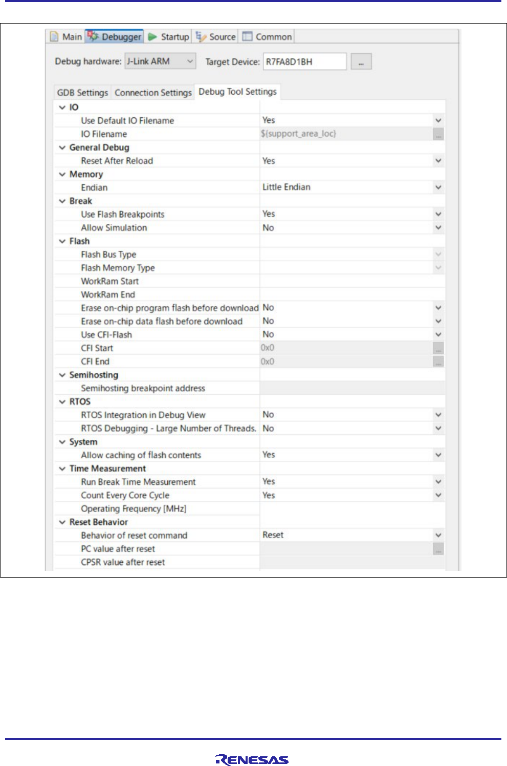
8.3 Appendix C: Debugger configuration

Renesas RA Family Quick Start Guide: EK-RA8D1 Modbus TCP
R20AN0737EJ0100 Rev.1.00 Page 17 of 20
Dec.11.23
Renesas RA Family Quick Start Guide: EK-RA8D1 Modbus TCP
R20AN0737EJ0100 Rev.1.00 Page 18 of 20
Dec.11.23

Renesas RA Family Quick Start Guide: EK-RA8D1 Modbus TCP
R20AN0737EJ0100 Rev.1.00 Page 19 of 20
Dec.11.23
Renesas RA Family Quick Start Guide: EK-RA8D1 Modbus TCP
R20AN0737EJ0100 Rev.1.00 Page 20 of 20
Dec.11.23
Revision History
Rev.
Date
Description
Page
Summary
1.00
Dec.11.23
-
First version

General Precautions in the Handling of Microprocessing Unit and Microcontroller
Unit Products
The following usage notes are applicable to all Microprocessing unit and Microcontroller unit products from Renesas. For detailed usage notes on the
products covered by this document, refer to the relevant sections of the document as well as any technical updates that have been issued for the products.
1. Precaution against Electrostatic Discharge (ESD)
A strong electrical field, when exposed to a CMOS device, can cause destruction of the gate oxide and ultimately degrade the device operation. Steps
must be taken to stop the generation of static electricity as much as possible, and quickly dissipate it when it occurs. Environmental control must be
adequate. When it is dry, a humidifier should be used. This is recommended to avoid using insulators that can easily build up static electricity.
Semiconductor devices must be stored and transported in an anti-static container, static shielding bag or conductive material. All test and
measurement tools including work benches and floors must be grounded. The operator must also be grounded using a wrist strap. Semiconductor
devices must not be touched with bare hands. Similar precautions must be taken for printed circuit boards with mounted semiconductor devices.
2. Processing at power-on
The state of the product is undefined at the time when power is supplied. The states of internal circuits in the LSI are indeterminate and the states of
register settings and pins are undefined at the time when power is supplied. In a finished product where the reset signal is applied to the external reset
pin, the states of pins are not guaranteed from the time when power is supplied until the reset process is completed. In a similar way, the states of pins
in a product that is reset by an on-chip power-on reset function are not guaranteed from the time when power is supplied until the power reaches the
level at which resetting is specified.
3. Input of signal during power-off state
Do not input signals or an I/O pull-up power supply while the device is powered off. The current injection that results from input of such a signal or I/O
pull-up power supply may cause malfunction and the abnormal current that passes in the device at this time may cause degradation of internal
elements. Follow the guideline for input signal during power-off state as described in your product documentation.
4. Handling of unused pins
Handle unused pins in accordance with the directions given under handling of unused pins in the manual. The input pins of CMOS products are
generally in the high-impedance state. In operation with an unused pin in the open-circuit state, extra electromagnetic noise is induced in the vicinity of
the LSI, an associated shoot-through current flows internally, and malfunctions occur due to the false recognition of the pin state as an input signal
become possible.
5. Clock signals
After applying a reset, only release the reset line after the operating clock signal becomes stable. When switching the clock signal during program
execution, wait until the target clock signal is stabilized. When the clock signal is generated with an external resonator or from an external oscillator
during a reset, ensure that the reset line is only released after full stabilization of the clock signal. Additionally, when switching to a clock signal
produced with an external resonator or by an external oscillator while program execution is in progress, wait until the target clock signal is stable.
6. Voltage application waveform at input pin
Waveform distortion due to input noise or a reflected wave may cause malfunction. If the input of the CMOS device stays in the area between V
IL
(Max.) and V
IH
(Min.) due to noise, for example, the device may malfunction. Take care to prevent chattering noise from entering the device when the
input level is fixed, and also in the transition period when the input level passes through the area between V
IL
(Max.) and V
IH
(Min.).
7. Prohibition of access to reserved addresses
Access to reserved addresses is prohibited. The reserved addresses are provided for possible future expansion of functions. Do not access these
addresses as the correct operation of the LSI is not guaranteed.
8. Differences between products
Before changing from one product to another, for example to a product with a different part number, confirm that the change will not lead to problems.
The characteristics of a microprocessing unit or microcontroller unit products in the same group but having a different part number might differ in terms
of internal memory capacity, layout pattern, and other factors, which can affect the ranges of electrical characteristics, such as characteristic values,
operating margins, immunity to noise, and amount of radiated noise. When changing to a product with a different part number, implement a system-
evaluation test for the given product.
・Arm
®
and Cortex
®
are registered trademarks of Arm Limited (or its subsidiaries) in the EU and/or elsewhere.
All rights reserved.
・Ethernet is a registered trademark of Fuji Xerox Co., Ltd.
・Modbus is a registered trademark of Schneider Electric, licensed to the Modbus Organization, Inc.
・Additionally all product names and service names in this document are a trademark or a registered trademark
which belongs to the respective owners. a trademark or a registered trademark which belongs to the respective
owners.

© 2023 Renesas Electronics Corporation. All rights reserved.
Notice
1. Descriptions of circuits, software and other related information in this document are provided only to illustrate the operation of semiconductor products
and application examples. You are fully responsible for the incorporation or any other use of the circuits, software, and information in the design of your
product or system. Renesas Electronics disclaims any and all liability for any losses and damages incurred by you or third parties arising from the use
of these circuits, software, or information.
2. Renesas Electronics hereby expressly disclaims any warranties against and liability for infringement or any other claims involving patents, copyrights,
or other intellectual property rights of third parties, by or arising from the use of Renesas Electronics products or technical information described in this
document, including but not limited to, the product data, drawings, charts, programs, algorithms, and application examples.
3. No license, express, implied or otherwise, is granted hereby under any patents, copyrights or other intellectual property rights of Renesas Electronics
or others.
4. You shall be responsible for determining what licenses are required from any third parties, and obtaining such licenses for the lawful import, export,
manufacture, sales, utilization, distribution or other disposal of any products incorporating Renesas Electronics products, if required.
5. You shall not alter, modify, copy, or reverse engineer any Renesas Electronics product, whether in whole or in part. Renesas Electronics disclaims any
and all liability for any losses or damages incurred by you or third parties arising from such alteration, modification, copying or reverse engineering.
6. Renesas Electronics products are classified according to the following two quality grades: “Standard” and “High Quality”. The intended applications for
each Renesas Electronics product depends on the product’s quality grade, as indicated below.
"Standard": Computers; office equipment; communications equipment; test and measurement equipment; audio and visual equipment; home
electronic appliances; machine tools; personal electronic equipment; industrial robots; etc.
"High Quality": Transportation equipment (automobiles, trains, ships, etc.); traffic control (traffic lights); large-scale communication equipment; key
financial terminal systems; safety control equipment; etc.
Unless expressly designated as a high reliability product or a product for harsh environments in a Renesas Electronics data sheet or other Renesas
Electronics document, Renesas Electronics products are not intended or authorized for use in products or systems that may pose a direct threat to
human life or bodily injury (artificial life support devices or systems; surgical implantations; etc.), or may cause serious property damage (space
system; undersea repeaters; nuclear power control systems; aircraft control systems; key plant systems; military equipment; etc.). Renesas Electronics
disclaims any and all liability for any damages or losses incurred by you or any third parties arising from the use of any Renesas Electronics product
that is inconsistent with any Renesas Electronics data sheet, user’s manual or other Renesas Electronics document.
7. No semiconductor product is absolutely secure. Notwithstanding any security measures or features that may be implemented in Renesas Electronics
hardware or software products, Renesas Electronics shall have absolutely no liability arising out of any vulnerability or security breach, including but
not limited to any unauthorized access to or use of a Renesas Electronics product or a system that uses a Renesas Electronics product. RENESAS
ELECTRONICS DOES NOT WARRANT OR GUARANTEE THAT RENESAS ELECTRONICS PRODUCTS, OR ANY SYSTEMS CREATED USING
RENESAS ELECTRONICS PRODUCTS WILL BE INVULNERABLE OR FREE FROM CORRUPTION, ATTACK, VIRUSES, INTERFERENCE,
HACKING, DATA LOSS OR THEFT, OR OTHER SECURITY INTRUSION (“Vulnerability Issues”). RENESAS ELECTRONICS DISCLAIMS ANY AND
ALL RESPONSIBILITY OR LIABILITY ARISING FROM OR RELATED TO ANY VULNERABILITY ISSUES. FURTHERMORE, TO THE EXTENT
PERMITTED BY APPLICABLE LAW, RENESAS ELECTRONICS DISCLAIMS ANY AND ALL WARRANTIES, EXPRESS OR IMPLIED, WITH
RESPECT TO THIS DOCUMENT AND ANY RELATED OR ACCOMPANYING SOFTWARE OR HARDWARE, INCLUDING BUT NOT LIMITED TO
THE IMPLIED WARRANTIES OF MERCHANTABILITY, OR FITNESS FOR A PARTICULAR PURPOSE.
8. When using Renesas Electronics products, refer to the latest product information (data sheets, user’s manuals, application notes, “General Notes for
Handling and Using Semiconductor Devices” in the reliability handbook, etc.), and ensure that usage conditions are within the ranges specified by
Renesas Electronics with respect to maximum ratings, operating power supply voltage range, heat dissipation characteristics, installation, etc. Renesas
Electronics disclaims any and all liability for any malfunctions, failure or accident arising out of the use of Renesas Electronics products outside of such
specified ranges.
9. Although Renesas Electronics endeavors to improve the quality and reliability of Renesas Electronics products, semiconductor products have specific
characteristics, such as the occurrence of failure at a certain rate and malfunctions under certain use conditions. Unless designated as a high reliability
product or a product for harsh environments in a Renesas Electronics data sheet or other Renesas Electronics document, Renesas Electronics
products are not subject to radiation resistance design. You are responsible for implementing safety measures to guard against the possibility of bodily
injury, injury or damage caused by fire, and/or danger to the public in the event of a failure or malfunction of Renesas Electronics products, such as
safety design for hardware and software, including but not limited to redundancy, fire control and malfunction prevention, appropriate treatment for
aging degradation or any other appropriate measures. Because the evaluation of microcomputer software alone is very difficult and impractical, you are
responsible for evaluating the safety of the final products or systems manufactured by you.
10. Please contact a Renesas Electronics sales office for details as to environmental matters such as the environmental compatibility of each Renesas
Electronics product. You are responsible for carefully and sufficiently investigating applicable laws and regulations that regulate the inclusion or use of
controlled substances, including without limitation, the EU RoHS Directive, and using Renesas Electronics products in compliance with all these
applicable laws and regulations. Renesas Electronics disclaims any and all liability for damages or losses occurring as a result of your noncompliance
with applicable laws and regulations.
11. Renesas Electronics products and technologies shall not be used for or incorporated into any products or systems whose manufacture, use, or sale is
prohibited under any applicable domestic or foreign laws or regulations. You shall comply with any applicable export control laws and regulations
promulgated and administered by the governments of any countries asserting jurisdiction over the parties or transactions.
12. It is the responsibility of the buyer or distributor of Renesas Electronics products, or any other party who distributes, disposes of, or otherwise sells or
transfers the product to a third party, to notify such third party in advance of the contents and conditions set forth in this document.
13. This document shall not be reprinted, reproduced or duplicated in any form, in whole or in part, without prior written consent of Renesas Electronics.
14. Please contact a Renesas Electronics sales office if you have any questions regarding the information contained in this document or Renesas
Electronics products.
(Note1) “Renesas Electronics” as used in this document means Renesas Electronics Corporation and also includes its directly or indirectly controlled
subsidiaries.
(Note2) “Renesas Electronics product(s)” means any product developed or manufactured by or for Renesas Electronics.
(Rev.5.0-1 October 2020)
Corporate Headquarters
Contact information
TOYOSU FORESIA, 3-2-24 Toyosu,
Koto-ku, Tokyo 135-0061, Japan
www.renesas.com
For further information on a product, technology, the most up-to-date
version of a document, or your nearest sales office, please visit:
www.renesas.com/contact/.
Trademarks
Renesas and the Renesas logo are trademarks of Renesas Electronics
Corporation. All trademarks and registered trademarks are the property
of their respective owners.
